
Digital chips are built from two kinds of logic. Combinational circuits compute a function of their present inputs only. Sequential circuits remember past inputs as state and compute from both the inputs and that state. The distinction looks elementary in a textbook, but it decides how you write RTL, how STA builds timing graphs, where clock domains and scan live in physical design, and what interviewers probe for.
This guide goes past definitions into timing, STA endpoints, PD implications and interview traps, with worked examples labeled illustrative.
Related reading: Latch vs Flip-Flop, CMOS Inverter, Static Timing Analysis, Setup and Hold Violations, Clock Gating and ICG, Time Borrowing and Multicycle Path and False Path.
Definitions that hold up in silicon
A combinational circuit is a network of gates (and wires) whose outputs at time t depend only on the inputs at time t, after the circuit’s propagation delay. There is no internal storage that remembers prior values. A 4:1 mux, a full adder, a priority encoder and a CLA adder are combinational. Glitches can appear on the outputs while inputs settle, but once the inputs are stable long enough, the outputs settle to a unique function of those inputs.
A sequential circuit has state: information stored in latches, flip-flops, memories or other regenerative elements. The outputs (and the next state) depend on the present inputs and the present state. Counters, shift registers, FSMs, pipelines and FIFOs are sequential. Without a clock or enable that advances or holds state, you cannot describe the behavior with a truth table alone.
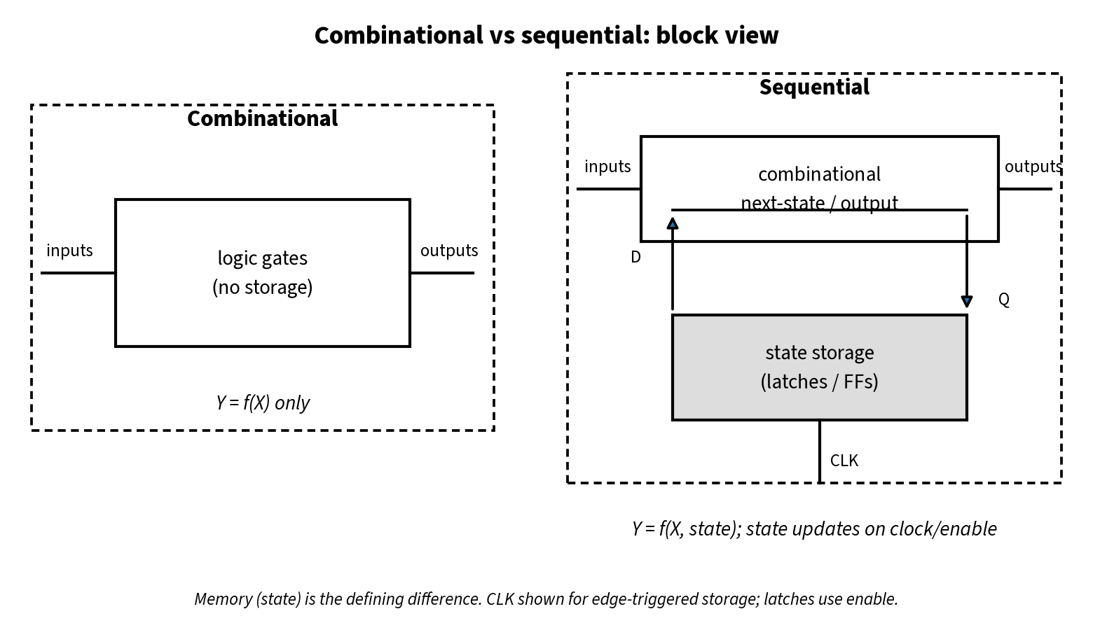
Memory is the dividing line. If removing every storage element leaves a pure gate cloud from primary inputs to primary outputs, the design was combinational. If state remains, it was sequential.
Truth tables versus state machines
Combinational logic is fully specified by a truth table (or Boolean equations, or a Karnaugh map). For n inputs there are at most 2^n rows. Synthesis maps that function onto library cells.
Sequential logic needs a state transition description:
- Present state and inputs determine next state.
- Present state (and, for Mealy machines, inputs) determine outputs.
You cannot flatten a non-trivial FSM into one truth table of the primary inputs alone, because the same input pattern can produce different outputs depending on history. That is why verification uses sequences and assertions, not only combinational equivalence of I/O cones.
Block view and everyday examples
In the classic block diagram, sequential logic is a combinational next-state/output cloud wrapped around a register file of state bits, with a clock (or latch enable) on the storage. Combinational logic is only the cloud—no feedback through storage.
| Aspect | Combinational | Sequential |
|---|---|---|
| Dependence | Present inputs only | Inputs + stored state |
| Storage | None (ideally) | Latches, FFs, RAM, etc. |
| Spec form | Truth table / Boolean | State diagram / HDL with regs |
| Clock | Not required for function | Required to update state (edge or level) |
| Typical blocks | Mux, adder, decoder, ALU combo | Counter, FSM, pipeline, FIFO |
| STA endpoints | I/O delays / virtual clocks | Launch and capture flops/latches |
| PD focus | Delay, slew, congestion of clouds | Clock tree, skew, domains, scan |
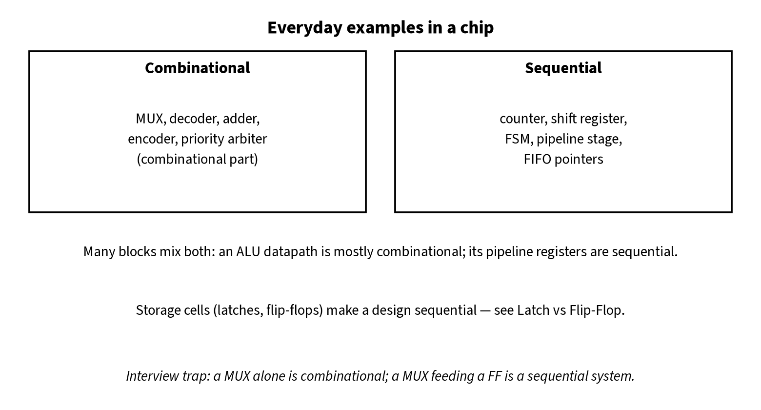
Examples (combinational): muxes and demuxes, binary adders and comparators, encoders/decoders, barrel shifters built from mux trees, combinational arbitration.
Examples (sequential): binary and gray counters, LFSRs, UART FSMs, CPU pipeline stages, synchronizer chains, clock-gated register banks.
Interview trap: “Is a mux sequential?” No—a mux alone is combinational. A mux whose select or data is registered, or that feeds a flop in a larger system, participates in a sequential design, but the mux cell itself has no state.
Latches and flip-flops: the storage that makes logic sequential
Storage in CMOS digital design is almost always latches (level-sensitive) or flip-flops (edge-triggered, often two latches in a master–slave pair). Both are sequential elements. The difference is when they sample and whether they are transparent.
- A positive latch is transparent while the enable is high: D flows to Q continuously in that window. Setup and hold are checked at the closing edge.
- A positive-edge flip-flop samples D on the rising edge of CLK and holds Q until the next rising edge. Setup and hold are checked at that active edge.
For the full comparison, timing windows and ICG latches, see Difference Between Latch and Flip-Flop. For PD and STA, remember: once you insert either element on a path, that path has sequential endpoints and clock-related checks.
Mealy and Moore (briefly)
Both Mealy and Moore machines are sequential—they have state registers.
- Moore: outputs are a function of state only. Outputs change when the state register updates (typically on the clock). Cleaner for timing isolation of outputs.
- Mealy: outputs are a function of state and inputs. Outputs can change as soon as inputs change, even mid-cycle. That can save a cycle of latency but creates combinational paths from inputs through output logic that STA must close like any other cloud.
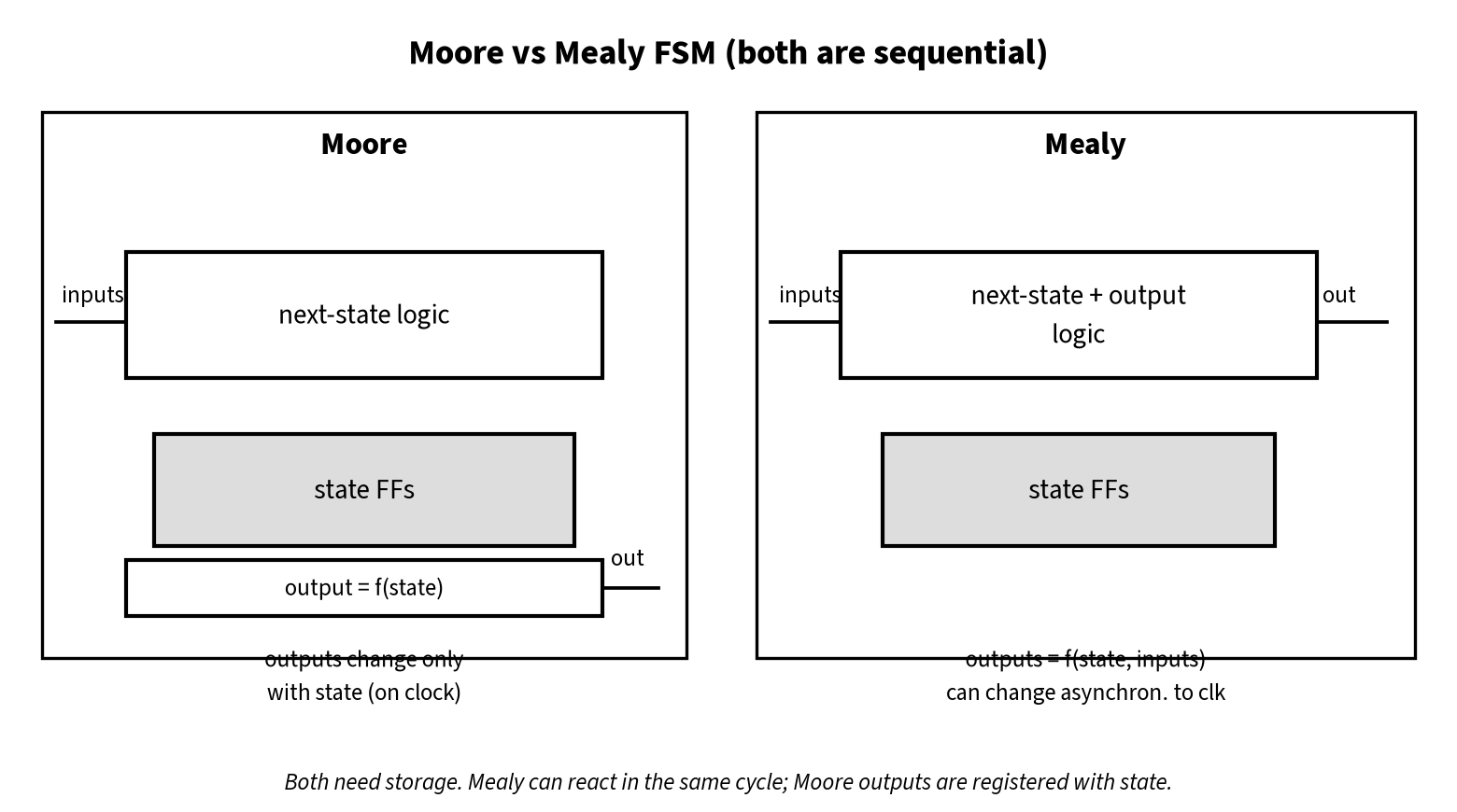
In practice, RTL often mixes styles: registered outputs (Moore-like) for chip interfaces, Mealy-like decode for same-cycle response inside a block. The classification matters less than knowing whether an output is registered.
Timing: propagation delay versus setup, hold and clock-to-Q
Combinational timing
For a combinational cloud, the number that matters is propagation delay from each input pin to each output pin (max for setup-critical paths, min for hold when that cloud sits between sequential elements). Libraries and STA also track transition (slew) and load. There is no setup/hold of the combinational cell itself in the flop sense—only pin constraints if the cloud is at the chip boundary.
If primary inputs change at time 0, outputs are valid after t_pd,max. Downstream logic must not sample those outputs earlier than that, which is why sequential elements enforce sampling windows.
Sequential timing
A flip-flop path between two registers on the same edge of the same clock (period T) obeys, in first-order form:
- Setup (max path): T ≥ t_cq + t_combo + t_setup − t_skew_useful
(skew and uncertainty refine the inequality; see your STA methodology). - Hold (min path): t_cq + t_combo_min ≥ t_hold + hold_skew_terms.
Here t_cq is clock-to-Q of the launch flop, t_combo is the combinational cloud between launch and capture, and t_setup / t_hold are capture-flop requirements. Pure combinational I/O has no T on an on-chip clock; you constrain it with set_input_delay / set_output_delay relative to a virtual or interface clock.
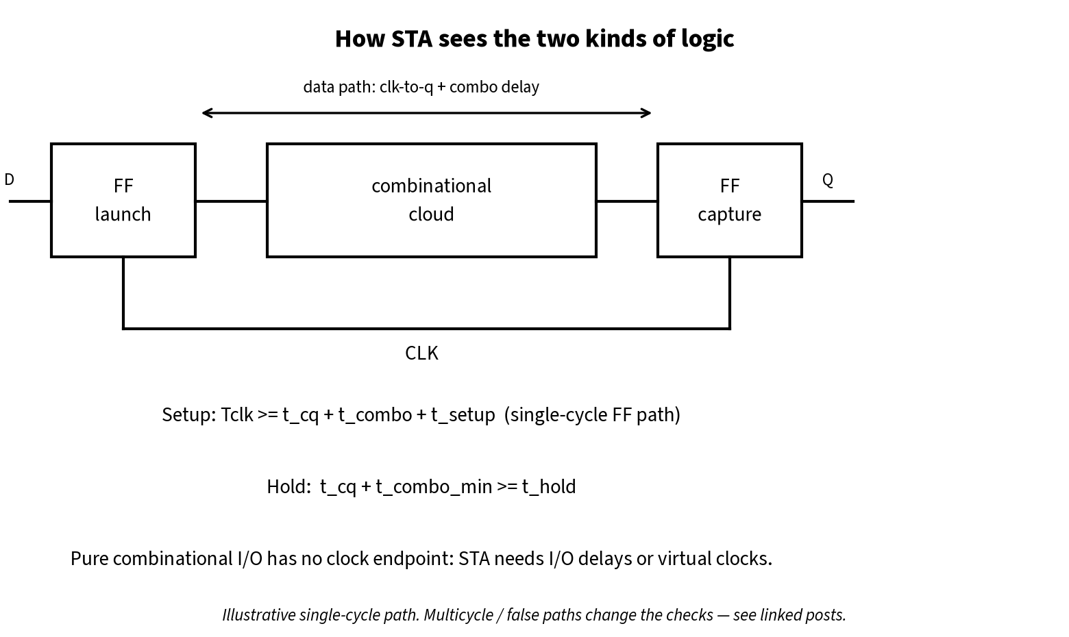
Worked example 1: single-cycle FF path (illustrative)
Assume T = 1.0 ns, t_cq = 80 ps, t_setup = 40 ps, clock uncertainty = 50 ps, and launch/capture skew = 0 for simplicity.
Required combo budget ≈ T − t_cq − t_setup − uncertainty = 1000 − 80 − 40 − 50 = 830 ps.
If the cloud’s max delay is 900 ps, setup slack is negative by 70 ps. Fixes are sizing, VT swap, buffering, logic restructuring, useful skew or a multicycle exception if functionally valid—not “making it combinational.”
Hold check (illustrative): t_cq,min = 40 ps, t_combo,min = 20 ps, t_hold = 30 ps → margin 40+20−30 = 30 ps. Removing combo delay (short path) can create hold fails; PD often inserts delay cells or detours.
Worked example 2: why “combinational only” chip pins still need clocks in STA (illustrative)
A pure combo block from port A to port Y has no flops. STA still needs a reference: define a virtual clock and set_input_delay / set_output_delay so that external setup/hold at the SoC level are modeled. Without that, there is no timed path—only unconstrained logic, which is a methodology fail, not “no timing.”
How STA treats combinational clouds versus sequential endpoints
Static timing analysis builds a timing graph of cells and nets. Sequential cells (flops, latches, memories) are timing endpoints (and startpoints): clocks are associated with them, and setup/hold (or latch time-borrow) checks are created. Combinational cells contribute delay and slew along arcs; they are not clocked endpoints by themselves.
Practical consequences:
- FF-to-FF (or latch) paths are the default timed fabric of a synchronous chip.
- Combo clouds appear as the delay between those endpoints. Optimizers resize and move cells inside the cloud; they do not invent clocks.
- I/O ports need delay constraints or they remain unconstrained.
- Exceptions—false paths, multicycle paths, clock groups—change which sequential relationships are checked. See Multicycle Path and False Path in STA.
- Latches enable time borrowing: a late arrival can still pass while the latch is open, with setup at the closing edge.
When a report shows a huge combo depth with no register break, either the path is real and needs pipelining/retiming, or a false path / case analysis is missing. Do not confuse “combinational path” in an STA report (the data arc between sequential points) with “the design has no sequential elements.”
Physical design implications
Placement density and combinational clouds
Deep combo cones create large soft clusters of standard cells with high local pin density and long critical wires. Congestion and IR drop can sit on those clouds even when the flops are sparse. Buffering trees and VT swaps are common ECO tools inside combo regions. Pipeline flops (sequential) break long paths but add area, clock load and latency.
Clock domains and sequential logic
Every flop or latch belongs to a clock domain (or is asynchronous). CTS, skew budgets, clock gating / ICG and CDC methodology exist because of sequential elements. Pure combinational islands between domains still need careful false-path or synchronized handshakes at the boundaries—the combo logic does not remove CDC risk if signals are sampled by unrelated clocks.
Scan and DFT
Scan chains stitch flops (and sometimes latches) into shift paths for manufacturing test. Combinational faults are observed through those sequential observation points. Scan reordering, lockup latches and scan hold are PD/DFT topics that only arise because the design is sequential. A purely combinational chip would use different test strategies (e.g., exhaustive or ATPG on combo cones with controllable I/O), which almost never matches modern SoC practice.
Power
Combinational switching energy scales with toggle rate and capacitance of the cloud. Sequential power adds clock power at every register—often a large fraction of dynamic power—which is why clock gating targets flops, not random combo gates.
Common interview traps
- “Sequential means slower.” Not necessarily. Pipelining (sequential) raises throughput; a huge combo cone can be the frequency limiter.
- “Latches are combinational because they are transparent.” False. Transparency is level-sensitive storage behavior; latches hold state when closed.
- “No clock in the RTL ⇒ combinational.” Always-on latches, SR latches inferred from loops, or memories can still create state. Check for inferred latches and feedback.
- “Truth table of a counter.” A counter needs state bits; a truth table of inputs alone is incomplete.
- “Setup/hold apply to AND gates.” Library setup/hold are for sequential pins (and some macros). Combo gates have delay arcs, not flop setup/hold.
- “Mealy is combinational.” Mealy output logic is combinational given state and inputs, but the machine as a whole is sequential because of state.
- Async resets and combo loops: unintended combo feedback can create latches or oscillation—STA and lint treat that as a sequential/design error.
Debugging flowchart: combo cloud or sequential path?
When a timing fail appears, decide what you are looking at before you resize cells at random.
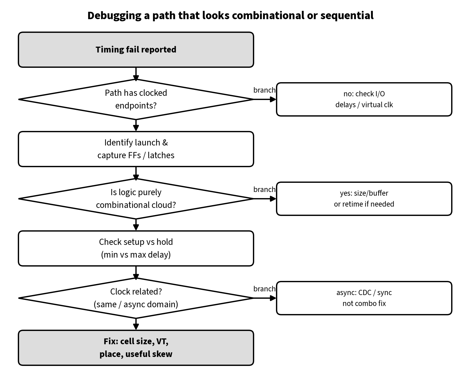
Checklist in words:
- Confirm whether the path has clocked start and end points.
- If not, fix I/O delays / virtual clocks before blaming cell delay.
- Separate setup (max) from hold (min).
- Check clock relationship (same edge, opposite edge, generated clock, async).
- Only then attack the combinational cloud (size, buffer, retime) or the clock path (skew, gating).
- For latch paths, check borrowing and closing-edge constraints.
RTL coding habits that encode the distinction
In SystemVerilog/VHDL, blocking assignments in combo always_comb / assign describe combinational clouds. Non-blocking assignments in clocked always_ff describe sequential updates. Mixing them incorrectly is a classic bug: a blocking assignment inside a clocked block can infer unintended combo behavior in simulation versus synthesis mismatches; an incomplete sensitivity or missing else in combo logic infers latches—accidental sequential elements.
Synthesis reports of inferred latches should be treated as defects unless you intentionally coded a latch-based design. Intentional latches need explicit library latch cells, proper enables and STA latch methodology. Accidental latches usually come from incomplete case/if assignments in combo processes.
Glitches, hazards and why sequential sampling matters
Combinational networks can produce static and dynamic hazards—temporary wrong values while multiple inputs or reconvergent paths switch. In a pure combo board-level LED driver that only needs a final settled value, a short glitch may be harmless. In a chip, if that glitch lands on a flop’s D input near the active edge, it can be sampled as a wrong state or cause setup/hold misery.
That is one reason synchronous design samples with flops: the cloud is allowed to glitch after the launch edge as long as D is stable through the setup window at capture. Asynchronous use of combo decode as a “clock” or reset is dangerous precisely because hazards become spurious edges. Prefer registered, glitch-filtered controls for clocks and resets.
Worked example 3: reconvergence glitch (illustrative)
Suppose Y = A & B, and A rises while B falls such that both are briefly 1 during skew between the two arrival times. Y can spike high even if the steady-state truth table says Y should stay 0 for the initial and final (A,B) pairs. A downstream flop with a tight hold or a narrow sampling window relative to that spike can capture a one. Fixing it is about path balancing, gray coding of selects, or registering the decode—not denying that the AND is combinational.
Asynchronous inputs and synchronizers
Real chips receive asynchronous signals relative to on-chip clocks. The first sampling flop can go metastable; a synchronizer chain (two or more flops) is sequential logic whose only job is to reduce the probability of propagating metastability. Treating an async input as a clean combinational primary input without synchronization is a functional and timing methodology error.
Comparison table (expanded checklist for reviews)
When reviewing RTL or a timing report, walk this checklist:
| Check | Combinational expectation | Sequential expectation |
|---|---|---|
| Lint | No inferred latches in combo blocks | Flops/latches match architecture |
| STA start/end | Ports with I/O delays | Clocked cells |
| CDC | N/A inside one cloud | Sync/FIFO/handshake at domain cross |
| DFT | Controllability via I/O or upstream regs | Scan stitch of regs |
| Power intent | Toggle of data nets | Clock gating of regs |
| ECO style | Resize/buffer/upsize VT in cloud | Move/resize regs, adjust skew, gate clocks |
Interview Q&As
Q1. What is the essential difference between combinational and sequential circuits?
A. Combinational outputs depend only on present inputs (after delay). Sequential outputs depend on inputs and stored state. State requires memory elements such as latches or flip-flops.
Q2. Is an FSM combinational or sequential?
A. Sequential. It has a state register. Next-state and output logic may be combinational clouds around that register (Moore/Mealy).
Q3. How does STA know where to apply setup and hold?
A. At sequential endpoints timed by clocks (flops, latches, sequential macros), subject to exceptions. Combinational cells contribute delay between those points.
Q4. Can a design with only muxes and adders still fail timing?
A. Yes. If those clouds sit between flops or at constrained I/O, their delay consumes the period or hold margin. Pure unconstrained combo with no delays specified fails methodology, not a period check.
Q5. Why do PD engineers care about this distinction?
A. Sequential logic drives clock tree, skew, CDC, scan and gating. Combinational clouds drive path delay, congestion and sizing ECOs. Retiming moves the boundary between the two.
Q6. Does clock gating turn sequential logic into combinational?
A. No. It stops or enables clock pulses to flops/latches to save power. State is retained; updates are suppressed. See Clock Gating and ICG.
FAQ
Can combinational circuits have feedback?
Intentional combo feedback without proper storage modeling creates asynchronous latches or hazards. Synchronous design avoids combo loops; use registered feedback for state.
Are ROMs and SRAM combinational?
Address decode and output muxing have combo delay, but bitcells store state—memory macros are sequential from a system view and have their own timing models (setup of address/controls, clocked reads/writes).
Where do setup and hold violations show up?
On sequential capture elements. The failing path’s data delay is often dominated by the combinational cloud. See Setup and Hold Violations.
Is pipelining always better?
Pipelining raises frequency and throughput at the cost of latency, area and clock power. It converts one deep combo path into shorter combo segments separated by flops.
Summary
- Combinational logic: Y = f(X); truth tables; delay and slew; no inherent clock.
- Sequential logic: state + f(X, state); latches/FFs; setup, hold, clk-to-Q; clocks and scan.
- STA times clouds between sequential endpoints (and constrained I/O). Exceptions reshape those relationships.
- PD cares about clocking, domains and scan for sequential parts and path delay/congestion for combo clouds.
- Interview clarity: storage ⇒ sequential; transparency ≠ combinational; Mealy/Moore are both sequential.
Master both views and you read STA reports, RTL and floorplans as one story—not as disconnected textbook chapters.
References
- Rabaey, Chandrakasan, Nikolić — Digital Integrated Circuits (logic styles, timing).
- IEEE / Accellera SDC concepts as implemented in major STA tools (clocks, input/output delay, exceptions)—consult your tool’s timing constraints guide.
- iVLSI: Static Timing Analysis
- iVLSI: Latch vs Flip-Flop
- iVLSI: Setup and Hold Violations
- iVLSI: Multicycle Path and False Path
- iVLSI: Time Borrowing
- iVLSI: Clock Gating and ICG
- iVLSI: CMOS Inverter