

Every digital chip is built from one idea: a pull-up network that connects the output to the supply and a pull-down network that connects it to ground, never both at once. The simplest example is the CMOS inverter, one PMOS and one NMOS transistor. Gate delay, slew, power, noise margins, latch-up and clock tree design can all be understood first on the inverter.
This guide covers the structure, working, VTC, noise margins, delay, power and layout of the inverter, and why it matters to PD and STA engineers.
Related reading: Physical Design Flow, Static Timing Analysis and Latch-up in CMOS.
Structure of a CMOS inverter
A CMOS (complementary metal-oxide-semiconductor) inverter uses two transistors of opposite type:
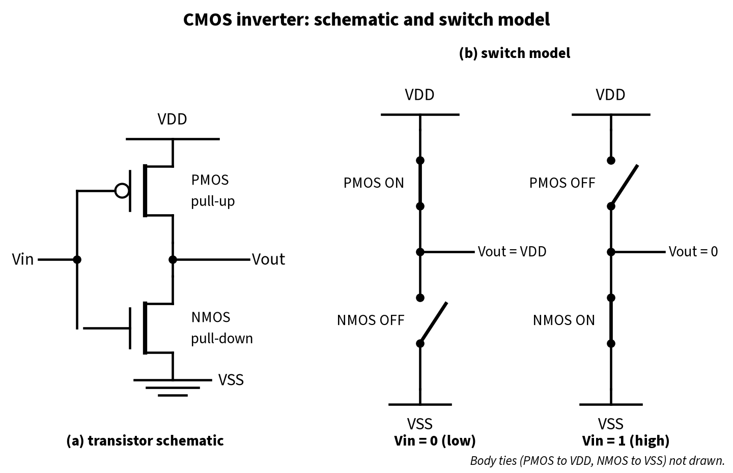
- A PMOS transistor (the pull-up) with its source on VDD and its drain on the output.
- An NMOS transistor (the pull-down) with its source on VSS (ground) and its drain on the output.
- The two gates are tied together and form the input. The two drains are tied together and form the output.
- The PMOS body (the N-well) is tied to VDD and the NMOS body (the p-type substrate or P-well) is tied to VSS, so the source-body junctions never forward bias in normal operation.
An NMOS turns on when its gate is high (VGS above its threshold voltage VTn). A PMOS turns on when its gate is low (VGS more negative than its threshold −|VTp|). Because the same input drives both gates, one transistor is on whenever the other is off. That is what “complementary” means.
How the CMOS inverter works
Think of each transistor as a switch controlled by the input:
- Input low (0 V). The NMOS is off. The PMOS has VGS = −VDD, so it is fully on and connects the output to VDD. Output = VDD (logic 1).
- Input high (VDD). The PMOS is off. The NMOS is fully on and connects the output to VSS. Output = 0 V (logic 0).
Three properties follow, and they are why CMOS replaced earlier logic families:
- Rail-to-rail output. The output connects through an on transistor to exactly VDD or VSS, so VOH = VDD and VOL = 0.
- Almost no static power. One transistor is always off, so there is no DC path from VDD to VSS; only leakage flows.
- Ratioless logic. Output levels do not depend on transistor sizes. Sizing changes speed and the switching point, not the logic levels.
Voltage transfer characteristic (VTC)
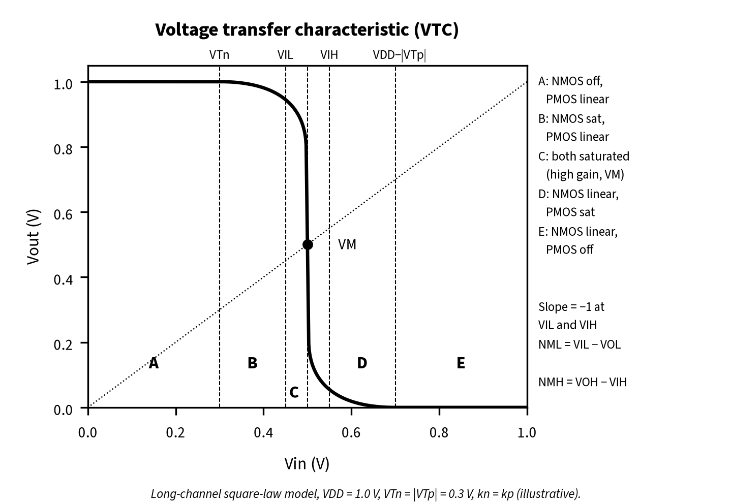
The VTC plots the output voltage against the input voltage as the input slowly sweeps from 0 to VDD. For a CMOS inverter it is a steep, S-shaped curve with five regions, named here A to E:
| Region | Input range (approx.) | NMOS | PMOS | Output |
|---|---|---|---|---|
| A | Vin < VTn | off | linear | VDD |
| B | VTn < Vin < VM | saturation | linear | slightly below VDD |
| C | Vin ≈ VM | saturation | saturation | falling very steeply |
| D | VM < Vin < VDD − |VTp| | linear | saturation | slightly above 0 |
| E | Vin > VDD − |VTp| | linear | off | 0 |
In region C both devices are saturated and the gain is very high. That gain makes logic regenerative: a slightly degraded input is restored to a clean rail, so noise does not accumulate through a chain of gates.
Switching threshold (VM)
The switching threshold VM is the point where Vin = Vout. In the simple long-channel (square-law) model, setting the NMOS and PMOS saturation currents equal gives:
VM = (VTn + r · (VDD − |VTp|)) / (1 + r), where r = √(kp / kn) and k = μ·Cox·(W/L).
- If kp = kn and VTn = |VTp|, then r = 1 and VM = VDD / 2. The inverter is symmetric.
- A stronger PMOS (larger r) moves VM up; a stronger NMOS moves it down.
Short-channel devices do not follow the square law, so use this for intuition and SPICE or the library for real numbers.
Worked example 1: switching threshold (illustrative)
Take VDD = 1.0 V and VTn = |VTp| = 0.3 V.
- With kp = kn: r = 1, so VM = (0.3 + 0.7) / 2 = 0.50 V.
- Now suppose the PMOS has half the strength of the NMOS (kp = 0.5·kn), for example because of lower hole mobility at equal width. Then r = √0.5 ≈ 0.707 and VM = (0.3 + 0.707 × 0.7) / 1.707 ≈ 0.795 / 1.707 ≈ 0.47 V.
A 2:1 strength mismatch moves VM by only about 30 mV, because VM depends on the square root of the strength ratio. Delay, which depends on strength directly, is far more sensitive.
Noise margins
Noise margins tell you how much noise a logic level can tolerate before the next gate misreads it. They are defined using the two points on the VTC where the slope is −1:
- VIL: the highest input voltage still treated as logic 0.
- VIH: the lowest input voltage still treated as logic 1.
- NML = VIL − VOL (noise margin for a low level).
- NMH = VOH − VIH (noise margin for a high level).
For CMOS, VOL = 0 and VOH = VDD in steady state, so the margins are large and, for a symmetric inverter, equal.
Worked example 2: noise margins of a symmetric inverter (illustrative)
For a symmetric long-channel inverter (kn = kp, VTn = |VTp| = VT, channel-length modulation ignored), the textbook results are VIL = (3·VDD + 2·VT) / 8 and VIH = (5·VDD − 2·VT) / 8.
With VDD = 1.0 V and VT = 0.3 V:
- VIL = (3.0 + 0.6) / 8 = 0.45 V
- VIH = (5.0 − 0.6) / 8 = 0.55 V
- NML = 0.45 − 0 = 0.45 V and NMH = 1.0 − 0.55 = 0.45 V
These match the VTC figure above, computed with the same model. Real margins are smaller: supply noise, IR drop and ground bounce shift the levels, and short-channel effects change the curve.
In physical design, noise margins appear as glitch analysis in signal integrity sign-off: a coupling glitch matters when it is large and wide enough to propagate through the receiver. See Crosstalk in VLSI.
Propagation delay and transition time
When the input switches, the output cannot change instantly. It has to charge or discharge the load capacitance CL through the on transistor. CL has three parts:
- The inverter’s own drain (diffusion) capacitance, its intrinsic load.
- The wire capacitance of the output net.
- The input (gate) capacitance of every fanout gate.
Two kinds of timing numbers describe the switching:
- Propagation delay: tpHL (output falling) and tpLH (output rising), measured from the input crossing its threshold to the output crossing its threshold, usually 50% of VDD. The average is tp = (tpHL + tpLH) / 2.
- Transition time (slew): how long the output takes to move between two thresholds, such as 10% to 90% or 20% to 80%. The thresholds are defined in the library.
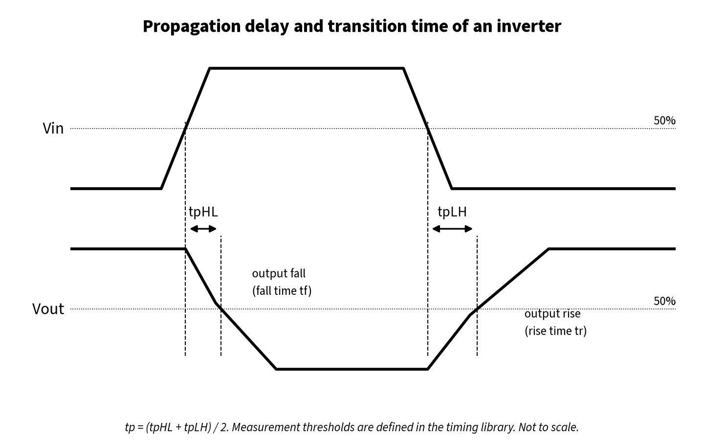
A first-order model treats the on transistor as an effective resistance Reff, giving tp ≈ 0.69 · Reff · CL (ln 2 for an RC step response). A stronger transistor has lower Reff.
Worked example 3: rise and fall delay (illustrative)
An inverter drives CL = 4 fF. Suppose its NMOS has Reff,n = 5 kΩ and its equal-width PMOS has Reff,p = 10 kΩ (the PMOS is weaker).
- tpHL ≈ 0.69 × 5 kΩ × 4 fF ≈ 13.8 ps
- tpLH ≈ 0.69 × 10 kΩ × 4 fF ≈ 27.6 ps
The rise is twice as slow as the fall. Doubling the PMOS width roughly equalizes them, but adds input capacitance and self-loading, so libraries choose the P/N ratio as a compromise (textbooks show minimum average delay at a smaller ratio than the one that equalizes rise and fall). Real delays come from the library.
How tools see an inverter’s delay
STA tools do not use Reff. They use the characterized timing library (see Timing Library (.lib)), where the delay and output slew of each cell are tabulated against input slew and output load (for example NLDM tables or current-source models). So:
- A slow input slew slows the output and lengthens the time both transistors conduct, one reason for max transition limits (see DRVs in VLSI).
- A large output load increases both delay and output slew, which then slows the next stage.
Delay also depends on supply voltage and temperature. A lower effective VDD from IR drop reduces drive current and increases delay. At low supply voltages, higher temperature can make cells faster rather than slower, the effect explained in Temperature Inversion in VLSI.
Sizing inverter chains
To drive a large load such as a long wire or a big clock net, a small inverter is too slow and a huge one overloads its own driver. The answer is a tapered chain of inverters, each a fixed factor larger than the last. The method of logical effort shows that a stage effort of about 4 gives close to minimum delay in typical processes, which is also why the FO4 delay (an inverter driving four copies of itself) is a common technology speed metric.
For example (illustrative), to drive a load 64 times the input capacitance of a unit inverter, the total effort is 64, and with a stage effort of 4 you need log₄64 = 3 stages, sized 1×, 4× and 16×, each driving a fanout of 4.
Power dissipation
A CMOS inverter dissipates power in three ways:
1. Dynamic (switching) power. Each time the output rises, the supply delivers energy CL·VDD². Half is stored on the load capacitor and half is dissipated in the PMOS; when the output falls, the stored half is dissipated in the NMOS. Averaged over time:
P_dyn = α · CL · VDD² · f
where α is the activity factor (the probability of a 0→1 output transition per clock cycle) and f is the clock frequency. The VDD² term is why voltage scaling is the most effective power lever.
2. Short-circuit power. While the input passes through the range VTn < Vin < VDD − |VTp|, both transistors conduct briefly and a direct current flows from VDD to VSS. It grows with slow input slews, another reason to keep transitions sharp.
3. Leakage (static) power. An off transistor still conducts a small current: subthreshold leakage (usually the largest part), plus gate and junction leakage. Leakage rises steeply with lower threshold voltage and higher temperature. Libraries therefore offer several threshold flavours (for example low-Vt fast and leaky, high-Vt slower and less leaky), and tools swap between them during optimization.
Worked example 4: dynamic power of one inverter (illustrative)
An inverter drives CL = 2 fF at VDD = 0.8 V and f = 2 GHz, with activity α = 0.1:
P_dyn = 0.1 × 2 fF × (0.8 V)² × 2 GHz = 0.1 × 2×10⁻¹⁵ × 0.64 × 2×10⁹ ≈ 0.26 µW
That looks tiny, but a design has millions of nodes, and a clock net has α = 1, ten times this example. That is why clock networks are a large share of dynamic power and why clock gating matters. See Power in VLSI for more.
Layout of a CMOS inverter
In a standard-cell library, the inverter is drawn as a cell of fixed height (measured in routing tracks) that abuts its neighbours in a row:
- A VDD rail runs along the top edge and a VSS rail along the bottom, shared with neighbouring cells.
- The PMOS sits in the N-well near VDD; the NMOS sits in the p-type substrate or P-well near VSS.
- A single gate line (polysilicon, or a metal gate in modern processes) crosses both active regions and forms both gates. The input pin connects to it.
- The sources connect to the rails, and the drains are joined by local metal to form the output pin.
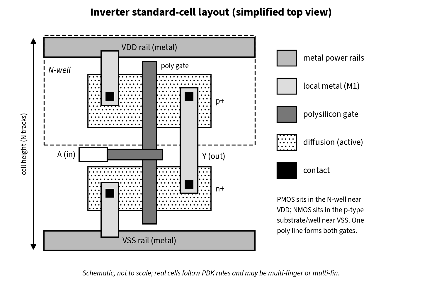
Larger drive strengths use multiple fingers in parallel. In FinFET processes width is set by the number of fins, so sizing is quantized.
Body ties, tap cells and latch-up
The N-well and substrate must be tied to VDD and VSS. Many modern libraries leave these ties out of the logic cells and rely on separate well-tap cells placed at a fixed maximum spacing; see Tap Cell Placement. The reason is latch-up: the p+ / N-well / p-substrate / n+ structure of every CMOS inverter forms a parasitic PNPN thyristor, and good, close taps keep its well and substrate resistances low. See Latch-up in CMOS.
Why the inverter matters in physical design
The inverter is not just a textbook circuit. PD and STA engineers meet it every day:
- Buffering and repeaters. Long nets are split by inverters or buffers to fix slew, capacitance and delay. A buffer is two inverters in series.
- Clock trees. CTS builds trees from clock buffers or inverters. Inverters are smaller and faster per stage, and because each swaps rising and falling edges, an inverter tree tends to balance rise/fall asymmetry, which helps duty cycle. See Clock Tree Synthesis and Duty Cycle and Pulse Width.
- Hold fixing. Delay cells built from inverter stages add delay on hold-critical paths. See Setup and Hold Violations.
- Sequential cells. Latches and flip-flops are built from inverters plus transmission gates or clocked inverters. See Latch vs Flip-Flop.
- ECOs. Spare inverters and buffers are common ECO spare cells.
Debugging a slow inverter or buffer stage
When STA reports a large delay on an inverter or buffer stage, the first-order model tells you where to look.
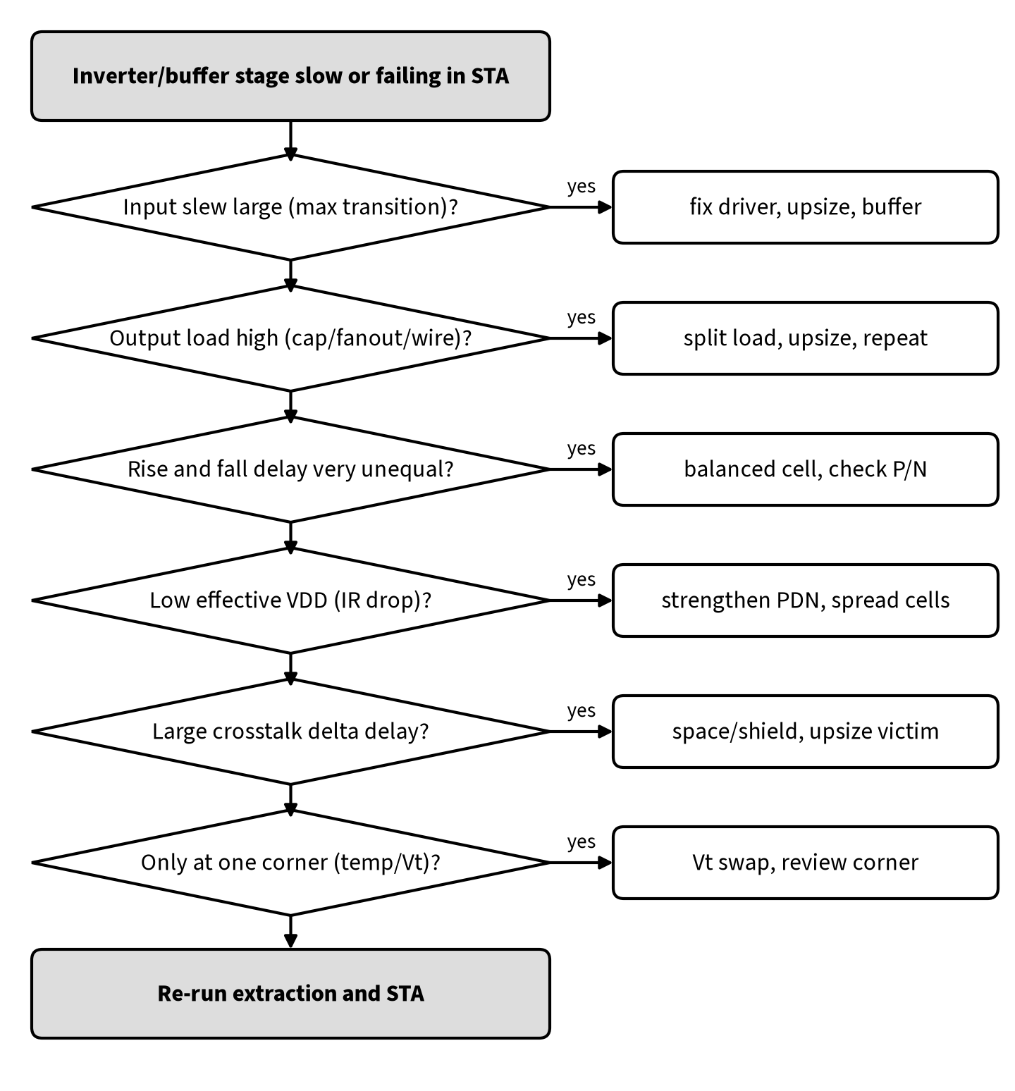
A practical checklist:
- Input slew. If the driving net has a large transition, fix the driver first (upsize, buffer or shorten the net).
- Output load. Check wire capacitance and fanout. Split the load, upsize the cell, or insert repeaters.
- Rise vs fall. A large imbalance points to a weak pull-up or pull-down; use balanced or clock-specific cells on clock paths.
- Effective supply. If the cell sits in a dynamic IR drop hotspot, fix the PDN or local density, not the cell.
- Crosstalk. A large delta delay means aggressor coupling. Space or shield the net, or upsize the victim driver.
- Corner. If it is slow at one corner only, consider a Vt swap and check temperature inversion coverage.
- Re-run extraction and STA to confirm the fix and catch new violations.
Interview questions and answers
1. What is a CMOS inverter?
A logic gate built from one PMOS pull-up and one NMOS pull-down with common gates (input) and common drains (output). It outputs the logical complement of its input.
2. Why does a CMOS inverter have almost no static power?
In either steady state one of the two transistors is off, so there is no DC path from VDD to VSS. Only leakage current flows.
3. What is the switching threshold VM?
The input voltage at which Vin = Vout. It depends on the relative strengths of the PMOS and NMOS; a symmetric inverter has VM = VDD/2.
4. Why is the PMOS usually wider than the NMOS?
Holes have lower mobility than electrons in most planar processes, so a PMOS of equal size has less drive current. Widening it balances rise and fall delay. In many FinFET processes the gap is smaller, so check the library’s P/N ratio.
5. Define noise margins.
NML = VIL − VOL and NMH = VOH − VIH, where VIL and VIH are the points on the VTC with slope −1. They measure how much noise a low or high level can tolerate.
6. What are the components of power in a CMOS inverter?
Dynamic switching power (α·C·VDD²·f), short-circuit power during input transitions, and leakage power.
7. How does input slew affect an inverter?
A slower input slew increases the propagation delay and output slew, and it lengthens the time both transistors conduct, increasing short-circuit power.
8. What is FO4 delay?
The delay of an inverter driving four identical inverters. It is a common, technology-normalized measure of gate speed.
9. Why do clock trees often use inverters instead of buffers?
An inverter is smaller and faster than a buffer, and alternating edge polarity tends to cancel rise/fall asymmetry. The tool must keep the inversion count to each sink correct.
FAQ
Do noise margins matter in standard-cell design?
You rarely compute them by hand, but they show up through glitch checks, IR drop and low-voltage operation, where margins shrink.
Summary
- A CMOS inverter is one PMOS pull-up and one NMOS pull-down sharing an input and an output; one transistor is always off in steady state.
- It gives rail-to-rail output, near-zero static power and ratioless logic levels.
- The VTC has five regions; at the switching threshold VM both transistors are saturated and the gain is highest.
- Noise margins are NML = VIL − VOL and NMH = VOH − VIH; a symmetric inverter has equal margins.
- Delay scales with load capacitance and transistor effective resistance; STA tools use library tables indexed by input slew and output load.
- Power has dynamic, short-circuit and leakage parts; P_dyn = α·C·VDD²·f.
- The inverter is the building block of buffers, clock trees, delay cells, flip-flops and spare cells.
References
- J. M. Rabaey, A. Chandrakasan and B. Nikolić, Digital Integrated Circuits: A Design Perspective, 2nd ed., Prentice Hall, 2003 (chapter on the CMOS inverter).
- N. H. E. Weste and D. M. Harris, CMOS VLSI Design: A Circuits and Systems Perspective, 4th ed., Addison-Wesley, 2010.
- I. Sutherland, B. Sproull and D. Harris, Logical Effort: Designing Fast CMOS Circuits, Morgan Kaufmann, 1999.
- S.-M. Kang and Y. Leblebici, CMOS Digital Integrated Circuits: Analysis and Design, 3rd ed., McGraw-Hill, 2003.