
The antenna effect in VLSI is a manufacturing reliability problem: during fabrication, long metal wires connected to a transistor gate can collect enough charge to damage the thin gate oxide. Physical design engineers must find and fix these antenna violations before tape-out, so the antenna check is a standard part of physical verification and sign-off alongside DRC and LVS.
In this tutorial we explain what causes the antenna effect, how plasma charging works, how the antenna ratio is calculated (with a worked example), the common antenna violation fixes – jumpers/layer hopping, antenna diodes and buffer insertion – how tools handle them, and the interview questions you are most likely to be asked.
What is the Antenna Effect in VLSI?
The antenna effect, also called plasma-induced gate oxide damage or process-induced damage, happens when a metal or poly conductor connected to a MOSFET gate acts like an “antenna” and collects charge during plasma processing steps. If that conductor is not yet connected to any diffusion (source/drain) that could drain the charge away, the charge can only discharge through the thin gate oxide. Too much charge causes a tunneling current that can degrade or break the oxide.
The damage may cause immediate failure, but it can also be latent: the transistor may work at test time but show threshold voltage shift, increased gate leakage or reduced lifetime later. That is why foundries enforce antenna rules strictly.
Why Does Plasma Charging Happen?
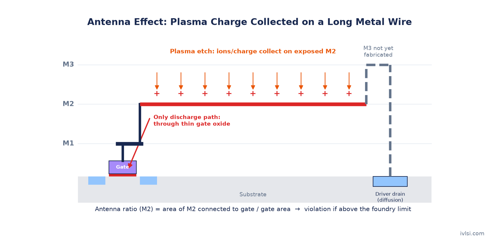
Metal layers are built one at a time. Steps such as plasma (reactive ion) etching of metal and via patterns and plasma-based deposition expose the wafer to charged ions and electrons. Exposed conductors collect this charge, and the amount collected grows with the conductor area (or perimeter, depending on the process and rule).
The key point is layer-by-layer fabrication. When metal 2 is being etched, metal 3 and above do not exist yet. So a gate that will eventually be connected to a diode or a driver’s diffusion through a higher metal layer is, at that moment, floating – connected only to the metal on the lower layers. Any charge collected on those lower-layer wires has only one discharge path: through the gate oxide.
Once the net is connected to a diffusion region (for example, the drain of the driving cell or an antenna diode), the charge has a safe path to the substrate, and further charging is no longer a concern for that net.
Factors that Increase Antenna Risk
- Long routes on a single lower metal layer that reach a gate before reaching any diffusion
- Small gate area (small input cells), since the same charge is concentrated on a smaller oxide
- Thinner gate oxides at advanced nodes
- Nets where the driver connects through a much higher layer than the receiver
- Long nets in routing of high-fanout or top-level signals
What is the Antenna Ratio?
Foundries express antenna rules using the antenna ratio: the ratio of the conductor area connected to a gate to the gate oxide area connected to that conductor.
Antenna Ratio (AR) = Area of conductor (metal/poly/via) connected to the gate
                     ---------------------------------------------------------
                     Total gate oxide area connected to that conductor
If the ratio exceeds the maximum allowed by the foundry rule deck, an antenna violation is reported. Rules are layer-specific and come in several flavours:
- Partial (per-layer) antenna ratio – considers only the area of one layer connected to the gate at the time that layer is processed.
- Cumulative antenna ratio – adds up the ratios (or areas) of the current layer and all lower layers connected to the gate.
- Area-based vs side-wall (perimeter) based – some rules use top area, some use side-wall area (perimeter × thickness), especially for metal etching.
- Diode-protected ratio – when a diode is connected, rules often allow a much larger ratio, sometimes as a function of diode area.
The exact formula, which layers are counted, and the limit values are defined in the foundry’s antenna rule deck (and in the LEF antenna properties used by the router). Always follow your technology’s rules – the numbers below are only for illustration.
Antenna Ratio: Worked Example
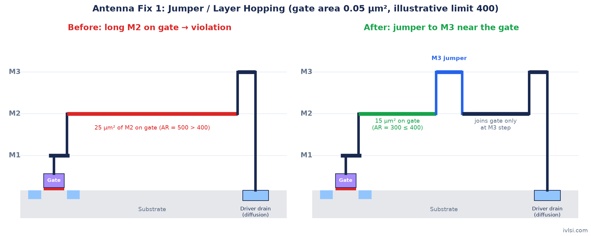
Assume a gate area of 0.05 µm² and an illustrative maximum partial ratio of 400 for metal 2. A net from driver D to receiver gate G is routed as follows:
| Segment | Layer | Area connected to gate G when the layer is etched |
|---|---|---|
| Pin access | Metal 1 | 2 µm² |
| Long horizontal route | Metal 2 | 25 µm² |
| Connection to driver | Metal 3 | –(driver diffusion connected only at M3) |
Step 1 – Metal 1 check: AR(M1) = 2 / 0.05 = 40 → OK.
Step 2 – Metal 2 check: during M2 etch, the gate is still floating (the driver connects only through M3). AR(M2) = 25 / 0.05 = 500 → exceeds 400, violation.
Step 3 – Fix with a jumper: the router breaks the M2 wire and hops up to M3 for part of the route, so only 15 µm² of M2 remains connected to the gate during M2 etch. AR(M2) = 15 / 0.05 = 300 → OK. The remaining M2 piece is connected to the driver side and joins the gate only when M3 is processed – by which time the driver’s diffusion is already connected and provides a discharge path.
Alternative fix: keep the routing and place an antenna diode near gate G. The diode gives a discharge path from the first metal layer, so the diode-protected rule applies instead.
Antenna Violation Fixes
1. Jumper / Layer Hopping
This is the most common and preferred fix. The long net segment on a lower layer is broken and routed through a higher metal layer for a short distance (a “jumper”). Since the upper layer is fabricated later, the lower-layer portion connected to the gate is reduced. Most routers prefer jumping up near the gate (receiver) pin so the gate sees as little lower-layer metal as possible. See Metal Layers and VIAs in VLSI for background.
Trade-offs: adds vias (resistance, via reliability) and upper-layer usage, which can affect congestion and timing slightly.
2. Antenna Diode Insertion
A reverse-biased diode (an antenna cell from the standard cell library, usually an N+/P-substrate diode) is connected to the net close to the gate input pin. During fabrication, the diode provides a leakage path that safely discharges plasma charge to the substrate. During normal operation, the diode stays reverse biased and has little effect apart from small added capacitance and leakage.
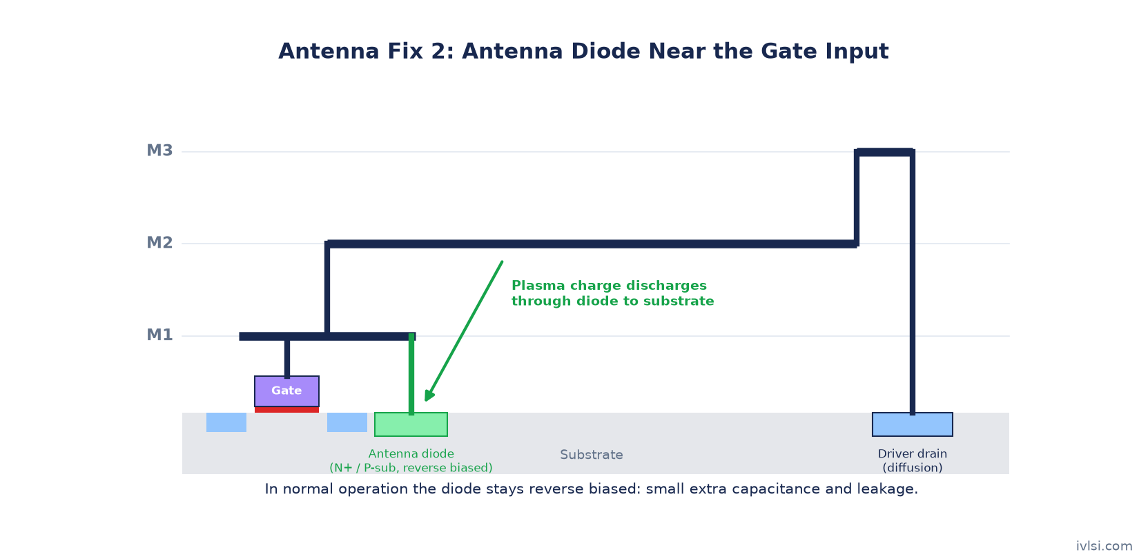
Trade-offs: needs placement space near the gate, adds capacitance (slightly more delay and power) and some leakage. Diodes are typically used when jumpers alone cannot fix the violation.
3. Buffer Insertion
Inserting a buffer (repeater) breaks the long net into two shorter nets. The gate of the original receiver now connects only to the short segment driven by the buffer output – whose drain diffusion provides a discharge path – and the buffer’s own input sees only the first half of the wire. This also helps transition and timing on long nets, but it changes the netlist, so timing must be re-verified.
4. Other Techniques
- Placing the driver close to the receiver so the net is shorter
- Routing the long part on the top layers from the start (layer assignment / non-default rules)
- Increasing gate area (e.g. using a larger input cell), which lowers the ratio
- Diodes at block ports – top-level nets entering a block may be unknown during block implementation, so antenna diodes are often added on input ports
| Fix | How it helps | Main cost |
|---|---|---|
| Jumper / layer hopping | Reduces lower-layer area connected to the gate | Extra vias, upper-layer resources |
| Antenna diode | Provides discharge path from early layers | Area, capacitance, leakage |
| Buffer insertion | Splits the net, driver diffusion discharges charge | Netlist change, power, timing re-check |
| Increase gate area | Lowers the ratio | Higher input capacitance |
How Tools Check and Fix Antenna Violations
Antenna rules are given to the implementation tool through the technology LEF (layer antenna rules such as ANTENNAAREARATIO, ANTENNACUMAREARATIO and diode-related factors) and cell LEF pin properties (ANTENNAGATEAREA for input pins, ANTENNADIFFAREA for output pins). The router uses them to avoid and repair violations during detailed routing. Final sign-off is done with the foundry antenna deck in the physical verification tool (for example Calibre or ICV), together with DRC and LVS.
A typical generic flow looks like this (exact command names differ between tools and versions, so check your tool’s documentation):
# 1. Ensure antenna rules are loaded (tech LEF / rule file)
# 2. Enable antenna fixing in the router (jumpers first, diodes second)
# 3. Run detail routing and route optimisation
# 4. Report antenna violations from the router
# 5. Fix remaining violations (ECO jumpers / diode insertion)
# 6. Run sign-off antenna check with the foundry deck in the PV tool
Scripting is useful for parsing antenna reports – see Regular Expressions in TCL and GREP Commands.
Antenna Effect Interview Questions
Q1. What is the antenna effect?
Charge collected on a long conductor connected to a gate during plasma processing, which can discharge through and damage the thin gate oxide.
Q2. Why is it a problem only during fabrication?
Because layers are built one at a time. During fabrication the gate may be floating until a higher layer connects it to a diffusion. After fabrication the driver’s diffusion always provides a discharge path.
Q3. Which fix is preferred – jumper or diode?
Usually jumpers (layer hopping), because they add no extra devices, leakage or capacitance. Diodes are used when jumpers are not enough or not possible.
Q4. Where should a jumper be placed?
Close to the receiver (gate) pin, so the gate sees minimum lower-layer metal.
Q5. Why are diodes placed close to the gate?
So that the diode connects to the net on the lowest layer and protects the gate from the earliest processing step.
Q6. Does the antenna diode affect the circuit in normal operation?
It is reverse biased, so the effect is small: some extra capacitance and leakage.
Q7. Can an antenna violation occur on an output pin net?
The concern is the gate oxide of the receiving input. A net that is already connected to the driver’s diffusion on the same or lower layers is protected.
Q8. What is the difference between partial and cumulative antenna ratio?
Partial considers only the current layer; cumulative adds the contribution of all lower layers connected to the gate.
FAQ
What is the antenna effect in VLSI?
It is gate oxide damage caused by charge collected on long metal or poly wires connected to a gate during plasma processing steps of chip fabrication.
What is the antenna ratio?
The ratio of conductor area connected to a gate to the gate oxide area. If it exceeds the foundry limit, an antenna violation is reported.
How do you fix antenna violations?
Mainly by layer hopping (jumpers to higher metal layers), adding antenna diodes near the gate, inserting buffers to split long nets, or re-routing long segments on upper layers.
Is the antenna check part of DRC?
It is usually run as a separate antenna deck in physical verification, alongside DRC and LVS, and many teams report it together with DRC.
Related iVLSI tutorials: Static Timing Analysis (STA) in VLSI | Setup and Hold Violations
Conclusion
The antenna effect is a fabrication-time reliability issue, but it must be solved during physical design. Understand why charge builds up layer by layer, calculate the antenna ratio correctly, and prefer jumpers before diodes or buffers. Continue with Routing and Pitch, Spacing & Offset to understand the routing context in which antenna violations are fixed.