
Tie cells are small standard cells that drive a constant logic 1 (tie-high) or logic 0 (tie-low) onto signal pins. They look trivial, but a missing, shared or wrongly powered tie cell can cause ERC and LVS failures, long noisy nets, power-domain bugs and painful ECOs. Interviewers like the topic because it tests whether you understand why the netlist and the silicon are not the same thing.
This guide covers why tie cells exist, what they look like inside, how synthesis and place and route insert them, fanout, multi-voltage and ECO rules, sign-off checks, a debug flowchart and interview Q&As. The worked examples are illustrative: the numbers show the method and are not taken from any foundry, library or project, except where an open-source library is named. Tool commands are simplified sketches; check your tool’s documentation for exact options. Related reading on iVLSI: Physical-Only Cells in VLSI, ECO in VLSI Physical Design, Power Gating in VLSI and LVS in VLSI.
What is a tie cell?
RTL is full of constants. A configuration bus is hard-wired (assign mode = 2'b01;), an unused input of an instantiated block is tied off, a mux select never changes in this product variant, or a spare gate needs its inputs held at a known value. After synthesis, each of these constant bits is still a net that some cell input pin reads, and every input pin in silicon must be driven by something.
A tie cell is that something. It is a standard cell with no logic inputs and one output (or two, in some libraries) that sits at a fixed logic level:
- Tie-high (TIEHI, TIE1, LOGIC1): output held at logic 1, close to VDD.
- Tie-low (TIELO, TIE0, LOGIC0): output held at logic 0, close to VSS.
The names vary by library. In the open Nangate45 library used by OpenROAD flows the cells are LOGIC1_X1 and LOGIC0_X1 with output pin Z. In the SkyWater SKY130 high-density library a single cell, sky130_fd_sc_hd__conb_1, provides both a HI and a LO output.
Why not connect inputs straight to VDD or VSS?
Logically, 1'b1 is VDD and 1'b0 is VSS, so why spend a cell on it? Three reasons.
1. Gate oxide reliability. A transistor gate tied directly to a supply rail sees every disturbance on that rail across its thin gate oxide, including supply bounce and, more seriously, electrostatic discharge (ESD) events that couple onto the power network. A tie cell puts a transistor channel between the rail and the load gates. The loads see a node that is held at the rail by a conducting transistor, not the rail itself, which limits the stress that reaches their oxide.
2. Rule decks and methodology checks. Because of that risk, many design methodologies and electrical rule checks (ERC) flag transistor gates connected directly to power or ground nets. If your netlist has a cell input wired to VDD, expect a violation that has to be fixed or explicitly waived.
3. Clean separation of power and signal nets. In place and route, VDD and VSS are special (power) nets built by the power grid, while tie nets are ordinary signal nets that the router, timing, noise and ECO tools all understand. Keeping constants on signal nets driven by real cells avoids odd special-net connections in the DEF and keeps LVS and the netlist in agreement. See Power Planning in VLSI for how the power grid itself is built.
What you must never do is leave an unused input floating. A floating CMOS input can drift to a mid-rail voltage, where both the pull-up and pull-down transistors of the receiving gate are partly on. That wastes static current and gives an unpredictable logic value. Tie it off.
Inside a tie cell
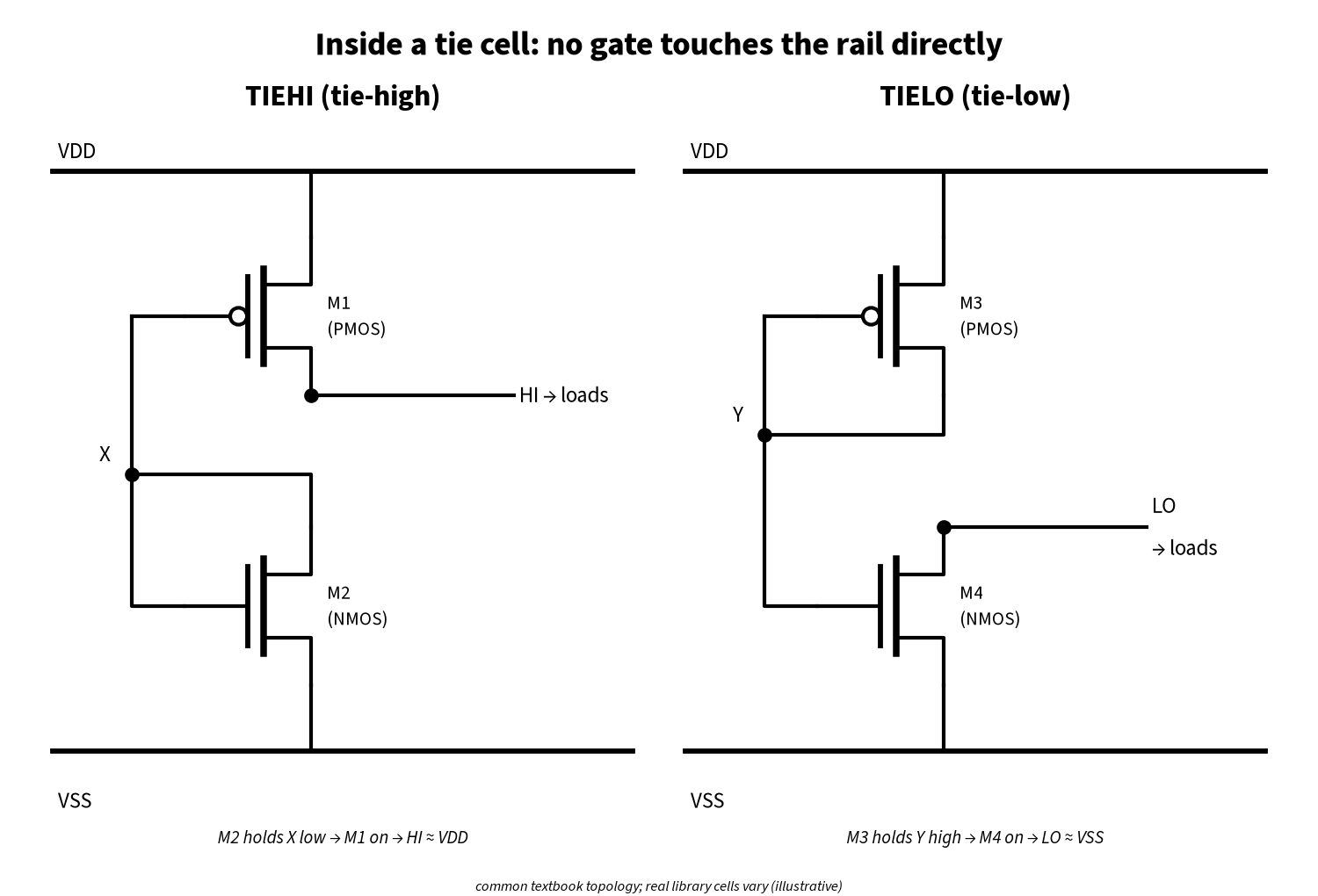
A common textbook tie-high uses two transistors. An NMOS (M2) is diode-connected: its gate and drain are tied together at node X and its source is at VSS, so it holds X low. X drives the gate of a PMOS (M1) whose source is at VDD, so M1 is on and its drain, the HI output, sits at VDD. The tie-low is the mirror image: a diode-connected PMOS holds node Y high, which turns on an NMOS that pulls the LO output to VSS. Real library cells vary, but the principle is the same: the output is driven through a transistor channel, and no gate in the cell or in the loads is wired directly to a rail.
How the library describes a tie cell
In Liberty, a tie cell is a cell with no input pins and an output pin whose function is a constant. The Nangate45 library, for example, defines LOGIC0_X1 with function : "0" on pin Z and LOGIC1_X1 with function : "1", each with VDD/VSS pg_pin definitions and an area of 0.532 µm². Both cells are also marked dont_touch : true and dont_use : true.
dont_usestops the synthesis or optimization engine from picking the cell as a general-purpose gate. Tie cells are inserted on purpose by a dedicated step, not chosen by the mapper.dont_touchstops optimization from sizing, removing or merging tie instances once they exist. Without it, an optimizer that sees “a constant net” might decide to restructure it in ways you do not want.
Tie cells normally have no timing arcs, because nothing switches. Most STA tools treat the constant function as a logic constant and propagate it, much like set_case_analysis, so arcs that can no longer toggle are disabled. That can block paths through gates whose side input is tied to the controlling value. Always check the tool’s constant-propagation reports, because a wrong constant can silently remove real paths from timing. See Static Timing Analysis (STA) in VLSI.
Where tie cells come from in the flow
Tie cells enter the design in two steps: synthesis maps constants to tie cells, and place and route makes the fanout physically sensible.
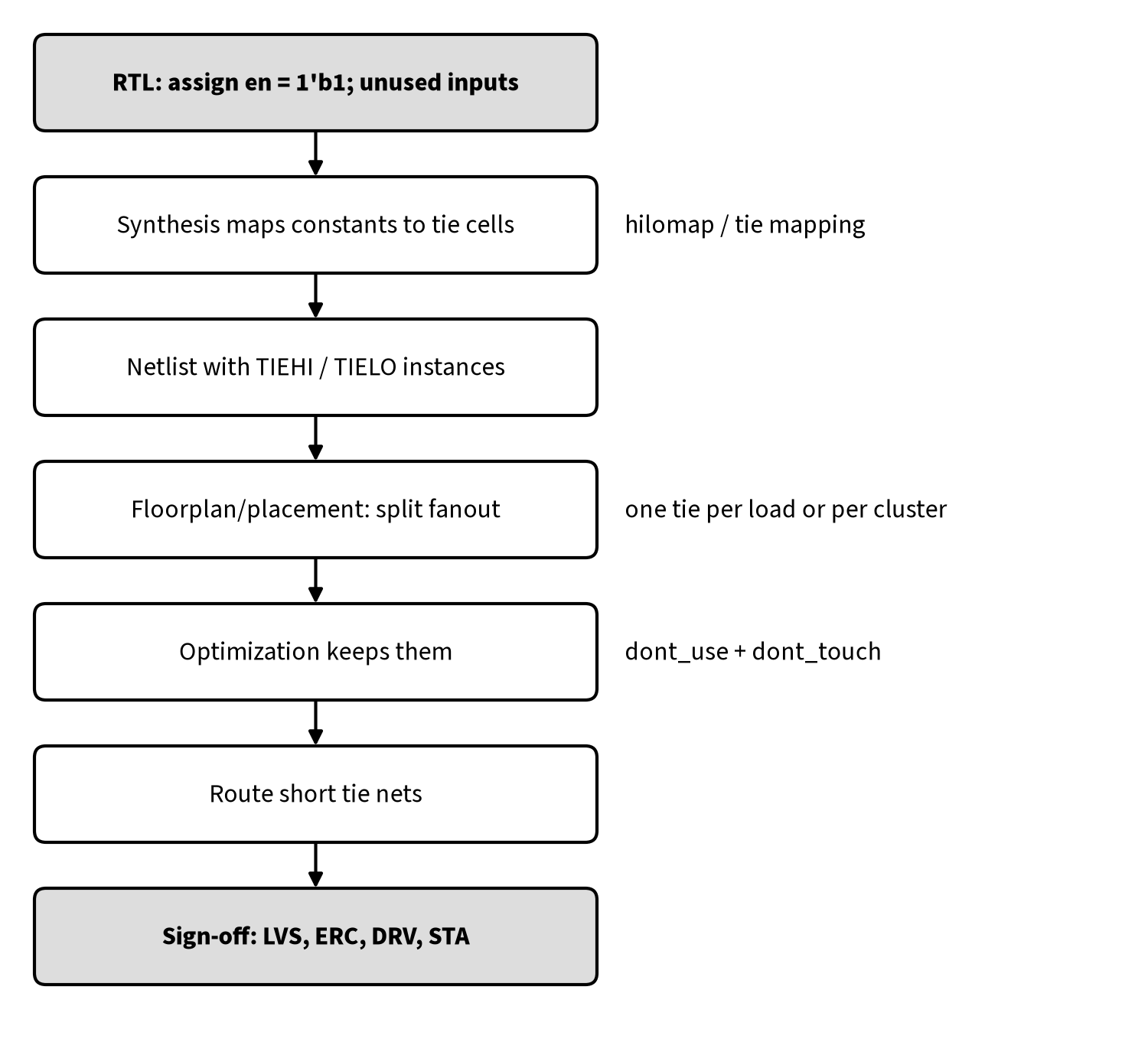
Synthesis. Each constant bit is connected to a tie cell. In the open-source Yosys tool this is the hilomap pass, which its help text describes as mapping constants to “tielo” and “tiehi” driver cells. By default it creates a separate cell for each constant bit; with -singleton it creates only one hi cell and one lo cell and connects every constant bit to them.
Floorplan or placement. A single tie cell per module is fine logically but bad physically, because its net would span the whole block. So place and route splits the fanout. In OpenROAD, the repair_tie_fanout command “connects each tie high/low load to a copy of the tie high/low cell”, with a -separation option that sets how far the new tie instance is placed from its load. OpenROAD also has an insert_tiecells command that inserts tie cells for a given master and port (for example LOGIC0_X1/Z). The OpenROAD-flow-scripts reference flow shows the typical combination: Yosys hilomap -singleton during synthesis, then repair_tie_fanout for the tie-low and tie-high cells at the floorplan step. A comment in that flow notes that tie fanout repair must run before buffer removal, because one tie cell may drive several buffers that drive several outputs.
# Synthesis (Yosys): map constants, one shared driver per value
hilomap -singleton -hicell LOGIC1_X1 Z -locell LOGIC0_X1 Z

# Floorplan (OpenROAD): give every tie load its own tie cell copy
repair_tie_fanout -separation 0 NangateOpenCellLibrary/LOGIC0_X1/Z
repair_tie_fanout -separation 0 NangateOpenCellLibrary/LOGIC1_X1/Z

# Generic STA/PnR Tcl sketch: count tie instances and inspect a tie net
sizeof_collection [get_cells -hierarchical -filter "ref_name =~ *TIE*"]
report_net [get_nets -of_objects [get_pins u_tie_12/Z]]
Commercial place-and-route tools offer the same controls (which cells, maximum fanout, maximum distance to load) under vendor-specific command names.
Fanout and placement rules
Two questions decide whether a tie implementation is clean: how many loads each tie cell drives, and how far away they are.
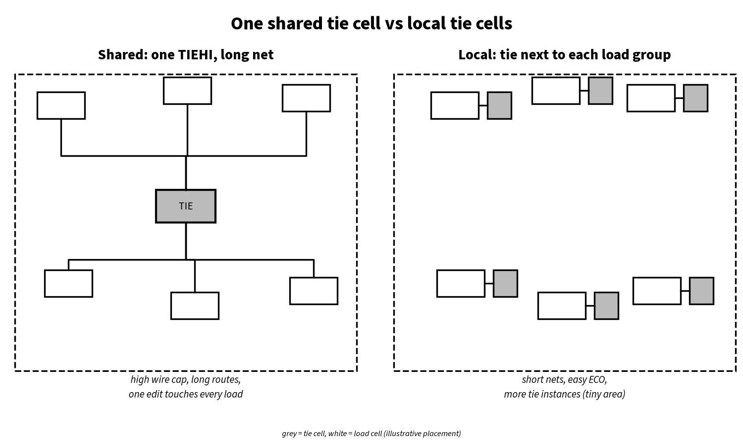
Keep tie nets short. A long tie net adds wire capacitance, uses routing tracks in possibly congested areas, and turns a weakly driven constant into a crosstalk victim. A glitch is dangerous on pins such as asynchronous set/reset, clock-gating enables or test-mode controls. Noise analysis should cover tie nets that feed such pins. See Crosstalk in VLSI.
Limit fanout. Many teams use one tie cell per load, or a small maximum fanout per tie cell, and a maximum distance between tie and load. Tie cells are tiny, and local nets let an ECO disconnect one load without touching the others.
Respect DRVs. If the library gives tie cells max_capacitance or max_fanout limits, a shared tie net will show up in the design rule violation report. Treat that as a placement problem, not as a reason to buffer a constant. See Design Rule Violations (DRVs) in VLSI.
Do not let optimization undo it. After placement optimization, CTS and routing, check that tie cells are still present, local and dont_touch.
Tie cells in multi-voltage designs
In a design with several power domains, a tie cell is powered by the supply of the domain it is placed in. That makes domain assignment part of correctness, not just neatness.
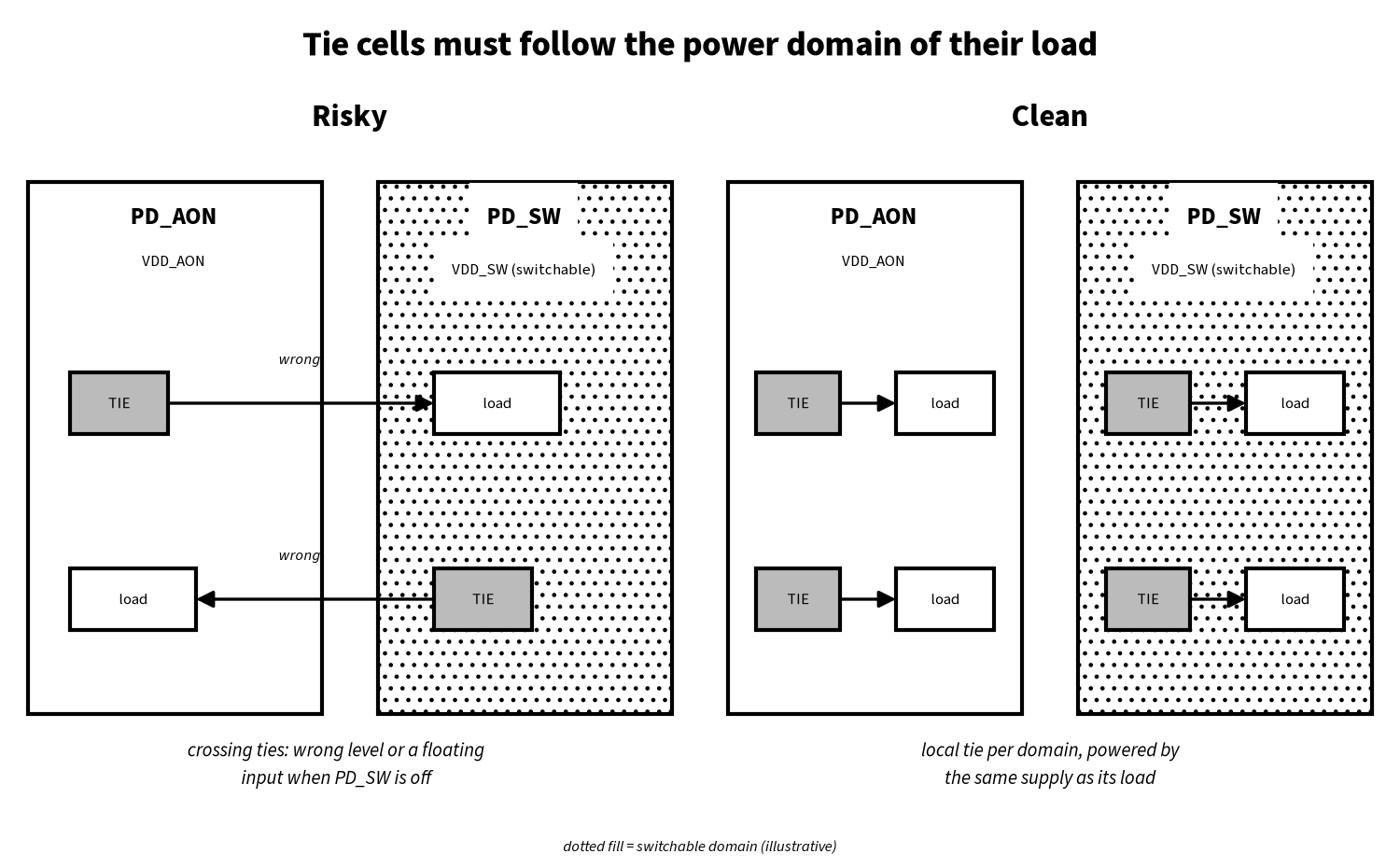
- Tie in a switchable domain driving an always-on load. When the switchable domain is powered down, the tie cell’s output is no longer driven, and the always-on input it feeds effectively floats. That is exactly the situation isolation cells exist to prevent, and it is unnecessary for a constant.
- Tie in one voltage domain driving a load in another. A tie-high at a lower supply driving a gate at a higher supply gives a logic 1 that is below the receiver’s supply. That can leave the receiver’s pull-up partly on and cost leakage, which is why level shifters exist for real signals. See Level Shifters in VLSI.
The fix is simple: place a local tie cell in the same domain as its load and connect it to that domain’s supplies. Low-power checks driven by UPF should confirm that no tie net crosses a domain boundary. See Power Gating in VLSI.
Tie cells, spare cells and ECOs
Spare cells are unused gates and flops spread across the die so that late fixes can be made by changing only metal layers. Their inputs must not float, so they are tied to constants through tie cells and their outputs are left open. In a metal-only ECO, you disconnect the spare cell inputs from the tie net and connect them to the real signals. If a single tie cell feeds many spare cells across a region, every one of those edits touches the same long net, and a reroute can create shorts or opens that LVS must catch. Local tie cells per spare cluster keep the edits contained. See ECO in VLSI Physical Design.
Sign-off checks that involve tie cells
- ERC: no gate pin connected directly to VDD or VSS; no floating inputs.
- LVS: tie cells are real devices; a tie cell missing from the exported netlist, or exported without power pins, causes mismatches. See LVS in VLSI.
- DRV and noise: tie nets within capacitance, fanout and length limits; glitch checks on sensitive pins.
- STA: constant propagation is intended and does not remove paths that should be timed.
- Low power: each tie cell in the same domain as its loads.
- Antenna and DRC: tie nets are ordinary signal nets with the same checks. See Antenna Effect in VLSI.
Worked examples (illustrative)
Example 1: from RTL constants to tie instances
Suppose a block contains assign cfg = 4'b1010; and instantiates a small IP whose unused test_en input is tied with .test_en(1'b0). That is five constant bits: two ones and three zeros.
- With Yosys
hilomap -singleton, synthesis creates one tie-high driving the two1bits and one tie-low driving the three0bits: 2 tie instances. - Without
-singleton, it creates one tie cell per constant bit: 5 tie instances. - After
repair_tie_fanoutat floorplan, each load pin gets its own copy, placed at the configured separation from its load, so you end with one tie cell per load pin whichever way synthesis started.
Count tie instances at each stage; a sudden drop after optimization usually means something removed them.
Example 2: one shared tie-low for 64 spare-cell inputs
A 400 µm × 400 µm block has 64 spare-cell inputs spread evenly, all tied low by a single TIELO placed at the centre. For loads spread uniformly over a square of side L, the average Manhattan distance from the centre is L/4 in x plus L/4 in y, which is L/2, or 200 µm here. Before any Steiner sharing, that is 64 × 200 µm, about 12.8 mm of routing on one constant net. Even with branch sharing, the net spans the whole block and couples to every signal it runs beside.
Now give each input a local tie cell a couple of microns away. The total tie routing drops to roughly 64 × 2 µm, about 0.13 mm, split into 64 isolated nets. The area cost, using the Nangate45 LOGIC0_X1 area of 0.532 µm², is 64 × 0.532 µm² ≈ 34 µm², which is negligible in a block of 160,000 µm². Wire lengths are illustrative; the area is the Nangate45 value.
Example 3: the tie that disappears at power-down
A tie-high in a switchable domain also drives the enable pin of an always-on cell. Simulation with the domain on passes, but at power-down the always-on cell sees an undriven input, and low-power checks report a missing isolation on what turns out to be a constant. The fix is not isolation but a local tie-high powered by the always-on supply.
Debugging tie-cell issues
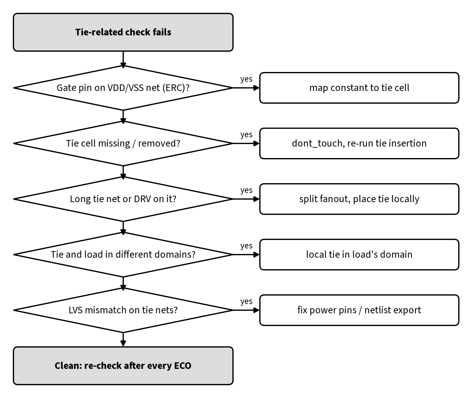
Work through the checks in order:
- Direct rail connections. Search the netlist for input pins on VDD or VSS nets. They usually come from a hand-edited netlist, an IP model or an ECO script that wrote
1'b1directly. Re-map them to tie cells. - Missing or removed tie cells. Compare tie-instance counts between synthesis, floorplan and post-route. Confirm
dont_touchon tie instances anddont_useon tie masters. - Long nets and DRVs. Report tie nets by length and fanout. Re-run fanout repair or tie insertion with a lower fanout or distance limit.
- Domain crossings. Check each tie net against the power intent. Replace crossings with local ties.
- LVS. If mismatches sit on tie nets, check that tie cells exist in the LVS netlist with correct power pins, and that the layout power connection to the tie cell is not open.
Interview questions and answers
Q1. What is a tie cell?
A standard cell with no logic inputs that drives a constant logic 1 (tie-high) or logic 0 (tie-low) onto signal pins, used wherever the netlist has a constant.
Q2. Why not connect a gate input directly to VDD or VSS?
Gate oxide reliability: a gate on the rail sees supply disturbances and ESD-coupled events directly. Tie cells put a transistor channel between the rail and the loads. Many ERC checks also flag gates tied directly to a supply.
Q3. Why are tie cells marked dont_use and dont_touch?
dont_use stops the mapper from using them as general logic; they are inserted by a dedicated step. dont_touch stops optimization from removing, merging or resizing them.
Q4. Why not use one tie cell for the whole block?
The net becomes long: more capacitance, more routing, crosstalk exposure and DRVs. ECOs become risky because every edit touches the same net. Local ties cost very little area.
Q5. Do tie cells have timing arcs?
Normally no. STA treats their constant output as a logic constant and propagates it, which can disable arcs downstream.
Q6. What care is needed in a multi-voltage design?
A tie cell is powered by its own domain. Place it in the same domain as its load; a tie in a switchable domain feeding an always-on load floats when powered down, and a tie at a different voltage gives the wrong level.
Q7. A tie cell drives an asynchronous reset pin. What would you check?
That the net is short, the tie cell is local and in the right domain, and noise analysis shows no glitch large enough to trigger the reset.
FAQ
Are tie cells physical-only cells?
No. Physical-only cells such as taps, endcaps, fillers and decaps have no logical function in the netlist. Tie cells drive logic values and appear in the netlist and in LVS as real logic cells. See Physical-Only Cells in VLSI.
When are tie cells inserted?
Constants are mapped to tie cells in synthesis; the fanout is then split and the cells placed near their loads during floorplan or placement, and checked again after optimization and ECOs.
Do tie cells consume power?
They do not switch, so they have no dynamic power; they contribute a small leakage like any cell.
Summary
Tie cells turn netlist constants into real, safely driven signals. They protect gate oxide by keeping load gates off the supply rails, keep ERC and LVS clean, and keep constants on ordinary signal nets that tools understand. Map constants in synthesis, split the fanout so each load or small cluster has a local tie cell, keep tie masters dont_use and instances dont_touch, place every tie cell in its load’s power domain, and re-check tie nets after every ECO. Do that and tie cells stay the boring cells they are supposed to be.
References
- OpenROAD documentation, Resizer (rsz) README, “Repair Tie Fanout” (
repair_tie_fanout): https://github.com/The-OpenROAD-Project/OpenROAD (openroad/rsz/README.md) - OpenROAD documentation, Initialize Floorplan (ifp) README, “Insert tieoff cells” (
insert_tiecells): https://github.com/The-OpenROAD-Project/OpenROAD (openroad/ifp/README.md) - OpenROAD-flow-scripts,
flow/scripts/synth.tcl,flow/scripts/floorplan.tcland platformconfig.mkfiles (TIEHI/TIELO settings for Nangate45 and SKY130): https://github.com/The-OpenROAD-Project/OpenROAD-flow-scripts - Yosys
hilomappass source and help text: https://github.com/YosysHQ/yosys/blob/main/passes/techmap/hilomap.cc - Nangate45 Open Cell Library Liberty file as shipped in OpenROAD-flow-scripts (
LOGIC0_X1,LOGIC1_X1): https://github.com/The-OpenROAD-Project/OpenROAD-flow-scripts/tree/master/flow/platforms/nangate45 - SkyWater SKY130 PDK documentation,
sky130_fd_sc_hd__conb: https://skywater-pdk.readthedocs.io/en/main/contents/libraries/sky130_fd_sc_hd/cells/conb/README.html