
A large SoC is rarely implemented as one flat netlist. It is split into partitions (blocks) that different engineers place, route and close in parallel, and then assembled at the top level. The catch is that a timing path does not stop at a block boundary. A path can start in a flop inside block A, leave through an output port, cross top-level routing and buffers, enter block B and end at a flop there. Someone has to decide how much of the clock period each piece of that path is allowed to use. That decision is time budgeting (also called timing budgeting or block budgeting).
Get the budgets right and blocks close independently and the top level comes together with little rework. Get them wrong and every block reports clean while the chip fails, or a block team spends weeks fighting a boundary path that was never feasible in the first place. This guide explains what a budget is, how it becomes block-level SDC, the common ways to split slack, how clocks and exceptions are handled, and how to debug budget problems, with illustrative worked examples, a flowchart, interview questions and an FAQ.
Related reading: Static Timing Analysis (STA) in VLSI, Standard Design Constraints (SDC), Setup and Hold Violations and Floorplan in VLSI Physical Design.
Why hierarchical designs need budgets
A flat run sees every path end to end, so the optimizer can spend slack wherever it is cheapest. In a hierarchical flow each block is implemented on its own, with only its own netlist and an abstract of its surroundings. Inside the block, flop-to-flop paths are fully visible and the chip-level SDC applies directly. The problem is the interface paths:
- Input paths: from a block input port to an internal register.
- Output paths: from an internal register to a block output port.
- Feedthrough (combinational) paths: from an input port straight to an output port with no register in between.
For each of these the block needs to know how much time the logic outside it will take, so it can work out how much is left for itself. The budget is exactly that information, written as constraints on the block’s ports. As the Omedes, Robert and Ramdani paper on block budgeting puts it, the budgeting step derives block I/O constraints from the chip constraints, and a good budget has to be feasible for each block and also guarantee that the chip constraints are met if every block meets its own.
What a budget looks like
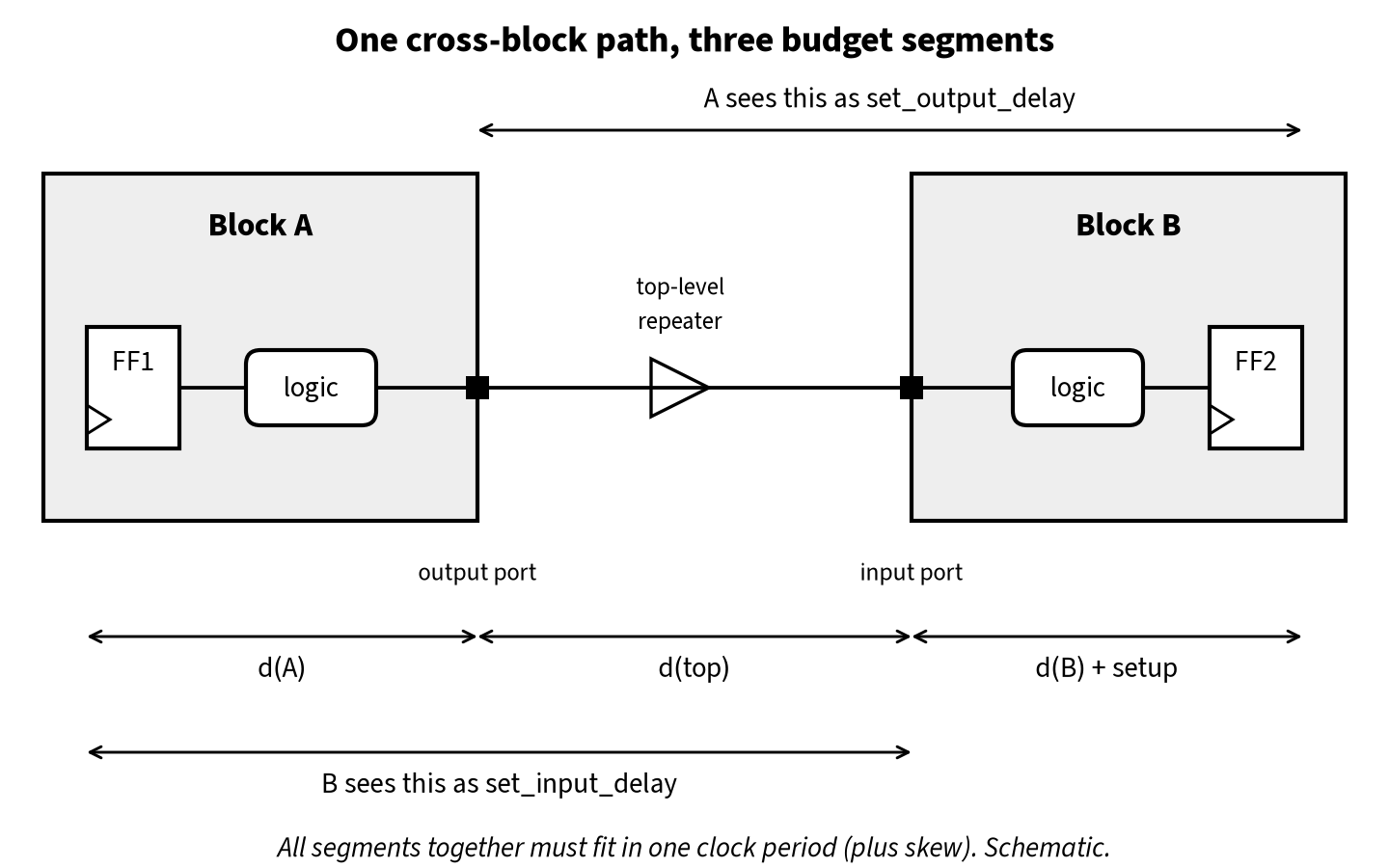
Take one cross-block setup path, clocked by the same clock at launch and capture, with period T. Split it into three segments: the part inside the launching block A, the top-level part (top routing, repeaters, any top-level logic), and the part inside the capturing block B. The basic budget condition is:
d(A) + d(top) + d(B) + setup time + margins ≤ T + (capture clock latency − launch clock latency)
Budgeting assigns each segment a share. Those shares are then expressed in SDC:
- For block A, the time left after A’s own segment is consumed by things outside A. That outside time becomes a
set_output_delayon A’s output port, referenced to the clock that captures the data. - For block B, the time already used before the data reaches B’s input port becomes a
set_input_delayon that port, referenced to the launching clock. - For a feedthrough, the allowed port-to-port delay is set with a
set_max_delaybetween the ports, or derived from the input and output delays together.
Budgets usually carry electrical context too, because a port delay alone does not tell the block how hard the outside world is to drive or how weak its drivers are:
set_driving_cellorset_input_transitionon inputs, so internal logic sees a realistic slew.set_loadon outputs, so the output driver is sized for the real top-level wire and fanout.- Port-related design rule limits such as
set_max_transitionandset_max_capacitance, which feed directly into DRV fixing.
Worked example 1: splitting one interface path (illustrative)
All numbers in this example are made up to show the arithmetic and do not come from any real process or library.
The clock period is 1,000 ps. Ignore clock skew for now and set aside 50 ps for setup time at the capture flop and 50 ps for uncertainty, which leaves 900 ps for data path delay.
An early estimate (from a flat trial run or a timing model) says the path needs about 300 ps inside A, about 150 ps on the top level, and about 250 ps inside B, a total of 700 ps. There is 200 ps of positive slack to share.
A proportional split gives each segment slack in proportion to its estimated delay:
| Segment | Estimate (ps) | Share of 200 ps slack | Budget (ps) |
|---|---|---|---|
| Inside A | 300 | 300/700 × 200 ≈ 86 | 386 |
| Top level | 150 | 150/700 × 200 ≈ 43 | 193 |
| Inside B | 250 | 250/700 × 200 ≈ 71 | 321 |
| Total | 700 | 200 | 900 |
Block A’s output port gets an output delay that covers everything after A: 193 + 321 = 514 ps of data delay plus the 100 ps of setup and uncertainty, so 614 ps. Block B’s input port gets an input delay of the launch clock-to-Q plus A’s and the top’s shares, here 386 + 193 = 579 ps (with clock-to-Q counted inside A’s segment). Each block now has a target it can close on its own, and if both meet it and the top-level route stays within 193 ps, the chip path closes.
In SDC form for block A, with illustrative port and clock names:
set_output_delay -clock CLK -max 614 [get_ports a_to_b_data*]
set_load 0.020 [get_ports a_to_b_data*]
And for block B:
set_input_delay -clock CLK -max 579 [get_ports a_to_b_data*]
set_input_transition 40 [get_ports a_to_b_data*]
Units in real SDC follow the library (often ns and pF), so check the units before copying any numbers.
Ways to divide the slack
There is no single correct split. The common strategies are:
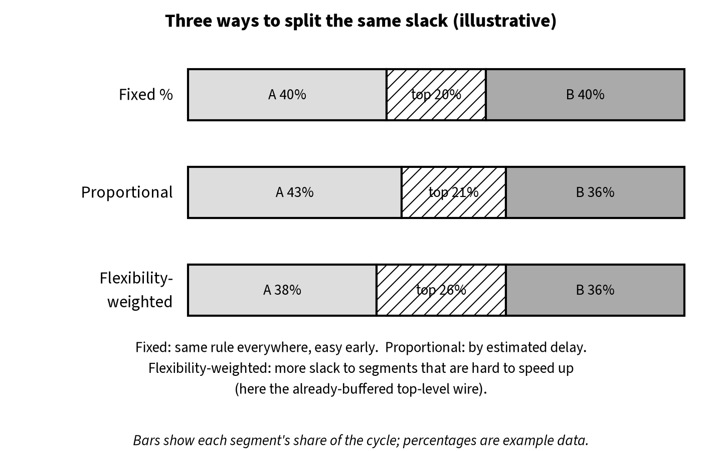
- Fixed percentage. The simplest rule: for example, give each block a fixed fraction of the cycle at each interface and the top level the rest. It is easy to apply early, before netlists are stable, but it ignores how much logic each segment actually has. A “half and half” split is a common starting point for register-to-register interfaces between two blocks.
- Proportional to estimated delay. As in the example above. It needs a delay estimate per segment, from a flat run, a prototype placement or timing models of each block.
- Weighted by flexibility. Some segments can be sped up cheaply (a short chain of small cells that can be upsized) and others cannot (a long top-level wire that is already optimally buffered, or a hard macro output). Budgeting research such as the Flexibility Aware Budgeting (FAB) approach in the paper above weights the slack distribution by how much each segment can still be optimized.
- Negotiated or iterative. Start from one of the above, implement, measure actual segment delays, and move slack from segments that closed with margin to segments that did not. Most projects end up here, whatever they start with.
A useful mental rule: budget the hard part first. If a top-level route across the die is long, compute its realistic buffered delay first and give it that, then split what is left between the blocks.
Handling clocks in budgets
Port delays are only meaningful relative to a clock, and clock treatment is where most budget bugs hide.
- Clock latency. In a hierarchical design the clock reaches the block through top-level clock tree segments. A block implemented with ideal clocks needs an estimate of the clock latency at its clock port, set with
set_clock_latency -sourceor similar, so the external timing is consistent with the real tree later. After CTS, the actual insertion delays at block ports should be fed back into the budgets. - Skew between blocks. If block B’s clock arrives later than block A’s, the cross-block setup path gains that difference and the hold path loses it. Budgets created before CTS should include a skew allowance in clock uncertainty, and the allowance should be revisited after the top-level clock tree is built.
- Virtual clocks. Port delays in block SDC are often referenced to a virtual clock that represents the clock at the other block. That keeps the block’s own clock tree from being mixed up with the external clock’s latency.
- Generated and divided clocks. If a block sees a clock divided at the top level, the budget must carry the generated clock definition, otherwise the block will time the interface at the wrong period.
Exceptions, hold and multi-mode
A budget derived only for single-cycle setup paths is incomplete.
- Timing exceptions. False paths, multicycle paths and max/min delay constraints in the chip SDC must be pushed down to the right block ports. A multicycle path that crosses a boundary has to be declared on both sides, or one block will over-optimize a path that has two cycles available. The US patent on budgeting nested partitions (US 8,977,995 B1) is a public example of a method that explicitly carries clock definitions, multicycle paths and path exceptions through the hierarchy.
- Hold budgets. Hold is checked with min delays. The block needs
-mininput and output delays as well as-max, so it does not leave an input-to-flop path so fast that it fails hold once the short top-level route is added. Hold fixing at the top usually costs less area than inside blocks, but only if the budget leaves room. - Modes and corners. A block may run in functional, scan shift and scan capture modes, each with its own clocks and constraints, and at several corners. Budgets need to exist per mode, and the sign-off corners used for budgeting should match the ones used for top-level STA.
- Latch-based interfaces. If a latch sits at the boundary, time borrowing changes the effective budget. See Time Borrowing (Cycle Stealing) for how to reason about it.
Where budgeting sits in the flow
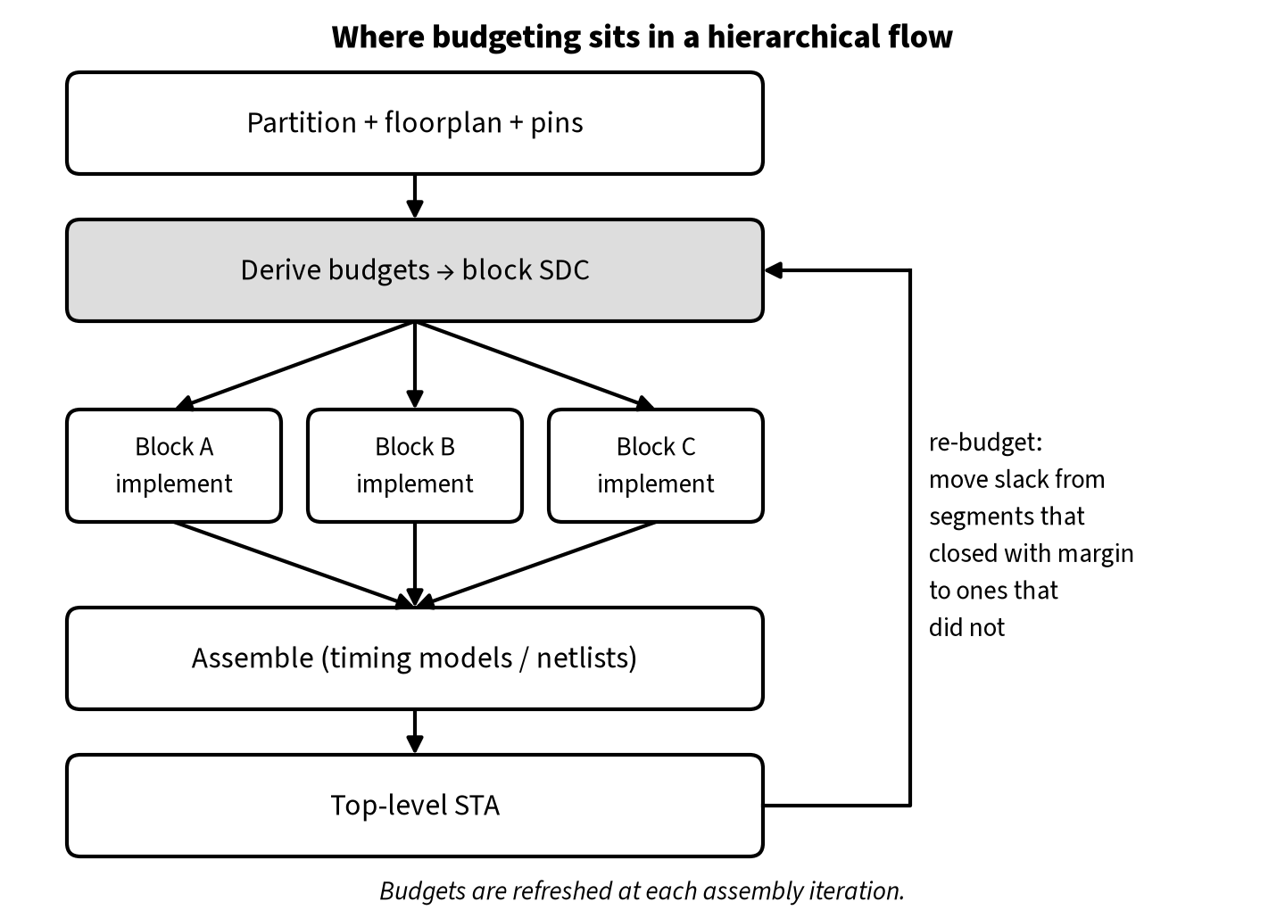
Budgeting is not a one-time step. A typical hierarchical flow uses it several times:
- After partitioning and floorplanning. Blocks, pins and top-level channels are placed. A first budget is derived from a flat trial timing run or from estimates, and block SDC is written out. Pin placement matters a lot here, because a badly placed pin forces a long route that eats the top-level budget.
- During block implementation. Each block closes timing against its own SDC.
- At assembly. Blocks are represented at the top level as timing models (for example extracted timing models or interface logic models) or as full netlists, and top-level STA checks the real interface paths.
- Re-budgeting. Slack measured at the top is redistributed, block SDC is updated and blocks run ECO or another pass. Each iteration should converge, so watch the trend in total negative slack of interface paths, not only the worst path.
Worked example 2: an over-constrained block (illustrative)
Again, all numbers are made up.
Block B reports a 120 ps setup violation on an input path from port cfg_bus[7] to a register. The internal path is only three cells and a short wire, and upsizing does not fix it. The engineer checks the input delay on the port: 820 ps on a 1,000 ps clock. Something outside B has been given 82% of the cycle.
Top-level STA on the assembled design shows that block A drives cfg_bus[7] directly from a flop, and the real delay from A’s clock pin to B’s port is about 450 ps. The budget was derived from an early estimate that assumed the signal went through a large top-level mux that was later removed.
The fix is re-budgeting, not optimization: the input delay on B’s port is reduced to a value based on the measured 450 ps plus a margin, A’s output delay on the same net is checked to make sure the two blocks still add up to the cycle, and the violation disappears without touching B’s netlist. This is the most common budget bug in practice: a stale estimate that nobody updated.
Worked example 3: a feedthrough path (illustrative)
A control signal enters block C and leaves again without a register, on its way from block A to block D. The total cycle available, after setup and uncertainty, is 800 ps. Block A uses 250 ps, the top-level routes into and out of C use 200 ps in total, and block D uses 150 ps. That leaves 200 ps for the path through C.
In C’s SDC this can be written as a port-to-port constraint:
set_max_delay 200 -from [get_ports ctl_in] -to [get_ports ctl_out]
or, equivalently, as an input delay and an output delay on the same clock that leave 200 ps between them. Feedthroughs deserve special attention in floorplanning: if C’s input and output pins for this signal are on opposite sides of a large block, 200 ps may not be enough for the wire alone. Moving the pins, or routing the signal around C at the top level instead of through it, is often a better fix than buffering.
Debugging budget problems
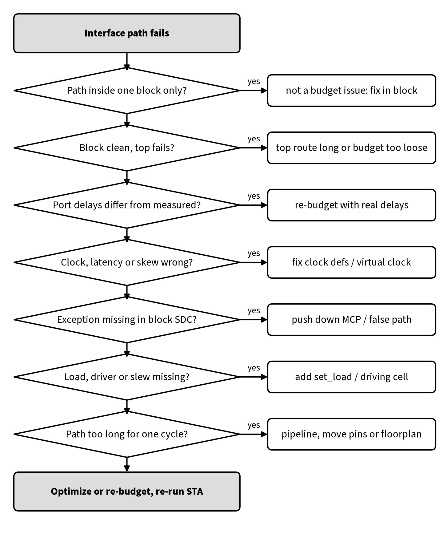
When an interface path fails, work through these checks before optimizing anything:
- Is it really an interface path? Confirm the path starts or ends at a block port in the block run, or crosses a block boundary at the top.
- Compare block slack with top-level slack. If the block is clean but the top fails, the budget was too generous to the block or the top-level route is longer than budgeted. If the block fails but the top passes, the budget was too tight for the block.
- Check the port delays against reality. Compare the input and output delays in block SDC with the delays measured at the top on the assembled design. Large differences mean a stale or wrong budget.
- Check the clocks. Confirm the right clock (real or virtual), period, latency and uncertainty are applied at the port, and that generated clocks are defined.
- Check exceptions. Look for multicycle or false paths in the chip SDC that did not reach the block, or block-level exceptions that do not exist at the top.
- Check electrical context. A missing
set_loador a wrong driving cell makes block timing optimistic at the ports. Compare port transitions in the block run with the top-level run. - Only then optimize or re-budget. If the total path cannot fit in the cycle whatever the split, the fix is architectural (pipelining, pin moves, floorplan changes), not a better budget.
Interview questions and answers
Q1. What is time budgeting in physical design?
It is the process of dividing the timing available on paths that cross block boundaries among the blocks and the top level, and writing those shares as block-level constraints (input and output delays, port-to-port max delays, loads and driving cells) so each block can be implemented independently.
Q2. Which paths need budgets?
Interface paths: input port to register, register to output port, and input port to output port (feedthrough). Register-to-register paths inside a block do not need budgets because the block sees them completely.
Q3. How are budgets expressed in SDC?
Mainly with set_input_delay and set_output_delay on ports, set_max_delay and set_min_delay for feedthroughs, plus set_load, set_driving_cell or set_input_transition, and the clock definitions, latencies and uncertainties the ports refer to.
Q4. A block is timing-clean but the top-level interface path fails. What do you check?
The block’s port delays against the delays measured at the top, the top-level route and buffering on the path, clock skew between the blocks, and whether any exception or load was missing in the block SDC. Usually the budget was too generous to the block or the top-level segment was underestimated.
Q5. Why do you need min (hold) budgets as well as max?
Because a block that only sees max delays may leave a very fast path from an input to a register. Once the short top-level connection is added, that path can fail hold. Min input and output delays let the block see the hold condition at its ports.
Q6. What is a virtual clock and why is it used in budgeting?
A clock with no source pin in the design, used as the reference for port delays. It represents the clock at the other end of the interface and keeps the external clock’s timing separate from the block’s own clock tree.
Q7. How does clock skew affect budgets?
If the capture block’s clock arrives later than the launch block’s, setup gains the difference and hold loses it. Budgets made before CTS should include a skew allowance, and the real insertion delays at block clock ports should be fed back after CTS.
Q8. What happens if a multicycle path is not pushed down to the block?
The block times the path as single-cycle, over-optimizes it, may report false violations, and wastes area and power. The exception must be declared consistently in the block and at the top.
Q9. When is re-budgeting better than fixing the path?
When the measured delays of the other segments are much smaller than budgeted. Moving that unused slack to the failing segment closes the path with no netlist change.
FAQ
Is budgeting needed for a flat design?
No. A flat run sees all paths end to end. Budgeting exists because a hierarchical flow implements blocks separately.
Is time budgeting done by the tool or by hand?
Implementation tools have budgeting commands that derive block constraints from chip-level timing, but engineers review, adjust and sometimes override the results, especially for critical interfaces and early in the project when estimates are rough.
How often should budgets be updated?
Whenever a block’s interface, pin placement, top-level routing or clock tree changes significantly, and at each assembly iteration. A stale budget is the most common cause of interface timing surprises.
Does a budget guarantee the chip will close?
Only if the budgets add up correctly for every interface path, every mode and corner, and the real top-level delays stay within their share. That is why top-level STA on the assembled design is always the final check.
Summary
- Time budgeting divides the timing of paths that cross block boundaries among the blocks and the top level.
- Budgets are written as block SDC: input and output delays, port-to-port max and min delays, loads, driving cells, and the clocks they refer to.
- Slack can be split by fixed percentage, by estimated delay, or by how much each segment can still be optimized; most projects iterate.
- Clock latency, skew, virtual and generated clocks, exceptions, hold and multiple modes all have to be carried into the budget.
- When an interface path fails, compare block and top-level results and check the port delays against measured delays before optimizing. Re-budgeting often fixes the problem without touching the netlist.
References
- O. Omedes, M. Robert and M. Ramdani, “Block Constraints Budgeting in Timing-Driven Hierarchical Flow,” DCIS 2004, Bordeaux, pp. 930-935: https://hal.science/lirmm-00108941v1
- US Patent 8,977,995 B1, “Timing budgeting of nested partitions for hierarchical integrated circuit designs”: https://patents.google.com/patent/US8977995B1/en
- US Patent 7,926,011 B1, “System and method of generating hierarchical block-level timing constraints from chip-level timing constraints”: https://patents.google.com/patent/US7926011B1/en
- Static timing analysis (overview): https://en.wikipedia.org/wiki/Static_timing_analysis