
If you have placed cells on a FinFET node, you have met cell-edge rules: certain cells cannot sit next to each other, some need a filler between them, and the legalizer sometimes refuses a location that looks perfectly empty. Much of that comes from how the edge of a cell’s diffusion is terminated. Two terms you will see in library documentation and interviews are PODE (poly on diffusion edge) and CPODE (often expanded as continuous or common poly on diffusion edge; naming differs between sources). Both are ways of ending one cell’s active region and isolating it from the next cell. They differ in how much space that isolation costs and in what rules they impose on placement.
This guide explains the concepts from a physical designer’s point of view: why diffusion must be broken at cell boundaries, what PODE and CPODE look like conceptually, how they relate to double and single diffusion breaks, and what they mean for placement, legalization, fillers and ECOs. Exact dimensions, spacings and rule names are foundry-specific and under NDA, so this article stays conceptual and uses only illustrative numbers.
Background: why cell edges need special treatment
In a FinFET (and gate-all-around) process, transistors are formed where gate lines (poly, later replaced by metal gate) cross the fins or sheets. Gate lines run on a fixed pitch across the whole row — the contacted poly pitch (CPP) — and cells are multiples of that pitch wide.
At the boundary between two cells, the fins of cell A and the fins of cell B are, physically, the same fins running across the row. Something must electrically break the diffusion so that the source/drain of the last transistor in cell A does not short to the first transistor in cell B. Also, the gate lines at the very edge of the cell are not real transistors; they are needed for regular patterning and process uniformity. They are dummy gates.
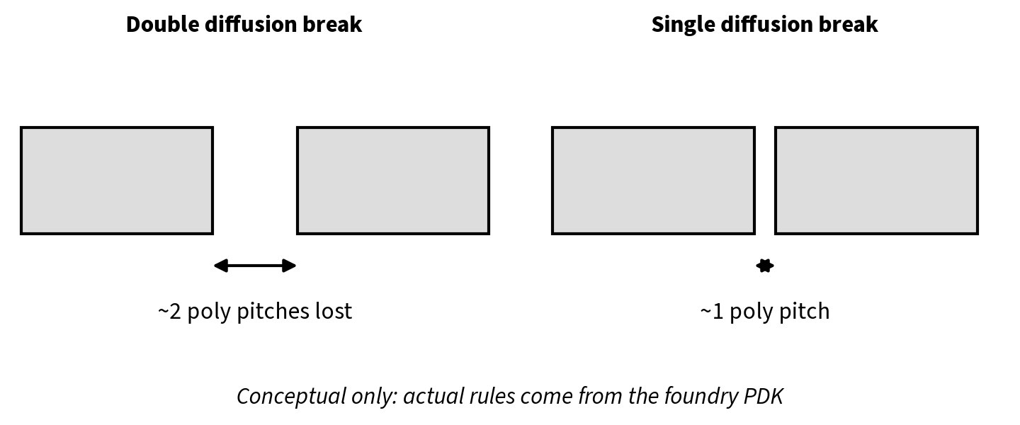
Two classic ways to end the diffusion:
- Double diffusion break (DDB): the fin is cut in a gap that spans roughly the width of two poly pitches between the two cells’ active regions. Each cell has its own dummy poly at its edge.
- Single diffusion break (SDB): the fin is cut under a single poly pitch at the boundary, so the isolation costs about one poly pitch instead of two.
PODE: each cell owns its edge poly
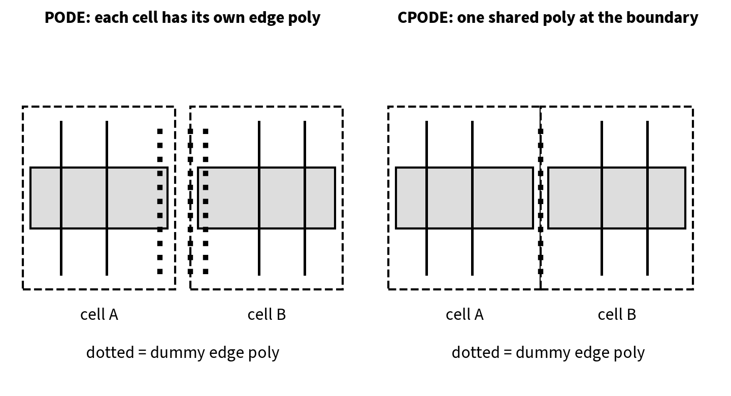
PODE places a dummy poly line on the diffusion edge of each cell. When two PODE cells abut, there is one dummy poly at the right edge of cell A and another at the left edge of cell B. The diffusion is isolated between them. Conceptually this behaves like a double-break arrangement: the isolation consumes space on both sides of the boundary.
Advantages:
- Each cell is self-contained, so any PODE cell can generally abut any other PODE cell (subject to other rules like Vt/implant edges).
- Layout and verification of the cell are simpler.
Cost:
- The isolation overhead is paid twice at every boundary — which adds up across a row of hundreds of cells.
CPODE: the boundary poly is shared
CPODE puts a single poly line exactly on the shared boundary. That poly is then processed (cut/removed and filled with dielectric, as public patent descriptions explain in general terms) so it acts as an isolation structure rather than a transistor. The two cells share one isolation line at the boundary, conceptually a single-break arrangement.
Advantages:
- Less isolation area per boundary, so rows can be denser. This is one of the techniques used to improve logic density at newer nodes.
Costs and complications:
- Abutment becomes a contract. Because the isolation is shared, both cells must have compatible edge types. Not every cell edge can abut every other cell edge.
- More edge rules. Libraries define edge types, and the technology defines which pairs can abut directly, which need a minimum spacing, and which need a specific filler or spacer.
- Mixed libraries. A design that mixes cells with different edge treatments needs transition rules between them.
Illustrative density arithmetic
All numbers are made up for teaching.
Assume a row of 200 cells, with an average cell width of 6 CPP including its edges.
- With a double-break style boundary costing 2 CPP total per boundary (1 CPP on each side), and a single-break style costing 1 CPP, the difference is about 1 CPP per boundary.
- 199 boundaries × 1 CPP ≈ 199 CPP saved in the row.
- Row length with double break ≈ 200 × 6 = 1200 CPP; with single break ≈ 1200 − 199 ≈ 1001 CPP.
That is about a 17% shorter row in this toy example. Real savings are smaller and depend on cell mix, how many boundaries need fillers anyway, and the actual rules; but the arithmetic shows why the industry cares about diffusion breaks — the cost is paid at every cell boundary.
What this means for placement and legalization
1. Edge-type aware legalization
The library defines edge types for left and right cell edges (in LEF/tech data or tool-specific rule files). The legalizer must check every left/right pair. That is why you can see a “legal” empty site rejected: the neighbours’ edges don’t allow that cell to sit there without a spacer.
2. Fillers and spacers are no longer just “fill”
At older nodes, fillers simply filled gaps to continue wells and rails. With edge rules, specific filler cells may be required between particular edge types, and some gaps have minimum widths. Filler insertion must follow the same rule set, or you will get DRCs at the very end.
3. Cell flipping and orientation
Flipping a cell (mirroring it about the Y axis) swaps its left and right edges. If the left and right edge types differ, a flip can make a previously legal abutment illegal. Detailed placement must consider orientation when checking edges.
4. Vt and implant boundaries
Cells of different threshold-voltage flavours use different implant layers, which have their own minimum-width and spacing rules at boundaries. Placing a single low-Vt cell between standard-Vt cells can create an implant island that is too small. Tools handle this by grouping same-Vt cells or inserting spacers, which interacts with the diffusion-edge rules.
5. Pin access
Denser rows mean pins of neighbouring cells are closer. Some flows add cell padding (keep-out space on cell sides) to improve pin access in congested regions; padding must also respect edge rules. See our congestion guide and placement interview questions.
6. ECOs
A late ECO that upsizes a cell or swaps its Vt can change its width or its edge type. If the new cell’s edges are incompatible with the neighbours, the ECO causes a cascade of shifts. Keeping some spare space or using ECO-friendly filler/decap cells near critical logic helps.
A debugging flow for edge-related legalization failures
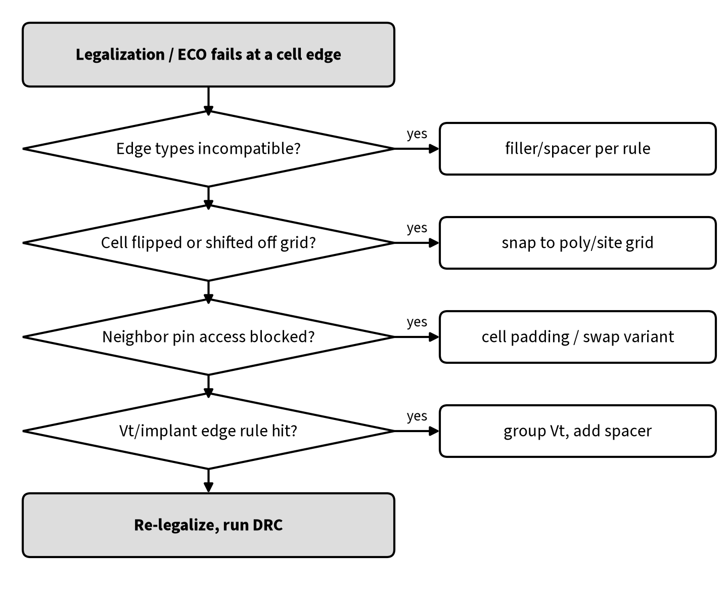
- Report the failing location and both neighbours’ edge types.
- If the edge pair is not allowed to abut, insert the required filler/spacer or move one cell.
- If the cell is off-grid or flipped, snap it to the site/poly grid and check orientation.
- If pin access is blocked, add padding or swap to a cell variant with different pin positions.
- If an implant/Vt rule is hit, group same-Vt cells or add spacers.
- Re-legalize and run DRC to confirm.
Representative legalization message
Messages differ by tool; this example is representative only:
WARNING: Cannot legalize instance u_alu/U1234 (NAND2_X2) at (102.336, 48.960)
  reason: edge spacing rule violation
  left neighbour  u_alu/U1180 right-edge type : EDGE_B
  this cell       left-edge type             : EDGE_A
  required spacing EDGE_B -> EDGE_A          : 1 site (or filler FILL_SP1)
  nearest legal location found               : (102.528, 48.960)
The fix is in the message: one site of spacing or the specified filler. When these warnings appear in thousands, the target utilization or cell mix is too aggressive for the edge rules, and you should revisit density in that region rather than fix them one by one.
PODE/CPODE vs other cell-edge concepts
| Concept | What it is | PD impact |
|---|---|---|
| PODE | Dummy edge poly owned by each cell | Simple abutment, more area per boundary |
| CPODE | Shared boundary poly used as isolation | Denser rows, edge-type abutment rules |
| Double / single diffusion break | How many poly pitches the isolation consumes | Area per boundary |
| Boundary / end-cap cells | Cells at row ends and macro edges | Required for well/edge integrity |
| Tap cells | Well/substrate ties at regular intervals | Placement grid constraints |
| Cell padding | Extra keep-out on cell sides | Pin access vs density |
Boundary/end caps and tap cells are separate requirements but are legalized by the same engines. See our CTS guide for how clock cells add their own placement constraints.
Common mistakes
- Running filler insertion with an old rule set. If the filler list or edge rules were copied from an older node or library, the final DRC will show edge violations everywhere.
- Ignoring orientation in custom placement scripts. Scripts that place or flip cells directly (for example, for datapath or clock structures) must check edges after the flip.
- Mixing libraries without transition rules. Combining cells from different library releases or vendors can introduce edge types that have no defined abutment rule.
- Fixing edge DRCs by hand after routing. Moving cells after routing creates new opens and shorts; fix edges at legalization time.
- Over-tight utilization in Vt-mixed regions. Many Vt swaps late in the flow create small implant islands that need spacers, which need space you no longer have.
Interview questions and answers
Q1. Why must diffusion be broken between standard cells in FinFET processes?
Fins run across the row, so without a break the source/drain of adjacent cells’ transistors would be electrically connected.
Q2. What is PODE?
Poly on diffusion edge: a dummy poly line at each cell’s diffusion edge, so each cell terminates its own active region.
Q3. What is CPODE?
A boundary poly shared by two abutting cells and processed into an isolation structure, so the cells share one break instead of each having their own.
Q4. What is the difference between single and double diffusion breaks?
A double break isolates over roughly two poly pitches; a single break over roughly one, saving area at every boundary.
Q5. Why can CPODE cause legalization failures?
Because abutment requires compatible edge types; incompatible pairs need spacing or specific fillers.
Q6. How does cell flipping interact with edge rules?
Flipping swaps left and right edges, which may make an abutment illegal.
Q7. Why are fillers more complex at advanced nodes?
Specific fillers may be required between certain edge types and must follow minimum-width and implant rules.
FAQ
Are PODE and CPODE foundry-specific terms?
They appear mainly in TSMC-related literature and patents; other foundries have similar concepts under different names. The underlying idea — how to isolate diffusion at cell boundaries — is universal.
Do I need to know the exact rules as a PD engineer?
You need to understand edge types and how your tool enforces them. The exact dimensions come from the PDK and library, under NDA.
Do GAA/nanosheet nodes still need diffusion breaks?
Yes. Sheets also run under gates and must be isolated at boundaries; the details change with the process.
Is CPODE the reason my utilization limit dropped?
Usually not directly — CPODE increases density — but the edge rules it introduces can reduce the effective utilization you can legalize, especially with mixed Vt and many cell types.
Summary
- Cells in FinFET/GAA rows share fins, so diffusion must be broken at boundaries.
- PODE gives each cell its own edge poly; CPODE shares one boundary poly as isolation, saving area per boundary.
- The density gain comes with edge-type abutment rules, required fillers and orientation constraints.
- Legalization, filler insertion, Vt grouping, padding and ECOs must all respect these rules.
- Keep rule numbers out of documents and training material; they belong to the PDK.