
Clock gating is the most widely used technique for reducing dynamic power in digital chips. The idea is simple: if a group of flip-flops does not need to change in a given cycle, stop their clock. The standard way to do this safely is with an Integrated Clock Gating (ICG) cell. In this tutorial we explain why clock gating saves power (with a worked calculation), why a plain AND gate is not safe, how an ICG cell works, clock gating setup and hold checks with numeric examples, how ICGs are handled in synthesis, placement and CTS, and common interview questions.
This post is a complete guide; for a shorter overview of the cell itself, see Integrated Clock Gating (ICG) Cell & Related Concepts.
Why Clock Gating? Dynamic Power Basics
Dynamic (switching) power of a node is approximately:
P_dynamic = α × C × V² × f

α = activity factor (switching probability per cycle)
C = switched capacitance, V = supply voltage, f = clock frequency
Data nets usually switch only part of the time, but the clock switches every cycle (α = 1 for its full transition pair), and the clock network drives a large total capacitance: every flip-flop clock pin plus the buffers and wires of the clock tree. That is why the clock network is a major contributor to dynamic power. Many registers, however, only load new data occasionally – think of a configuration register or a pipeline stage that is idle most of the time. Clocking them every cycle wastes power even when their data does not change.
Worked Example: Power Saved by Clock Gating
Assume (illustrative values) a register bank whose flip-flop clock pins plus local clock wiring add up to C = 50 fF, at V = 0.8 V and f = 1 GHz, and the bank only needs to load data in 25% of cycles.
Without gating: P = 1 × 50 fF × (0.8 V)² × 1 GHz = 50×10⁻¹⁵ × 0.64 × 10⁹ = 32 µW.
With gating: the clock reaches the bank only in 25% of cycles, so P ≈ 0.25 × 32 µW = 8 µW, plus the small overhead of the ICG cell itself, which is still clocked every cycle.
The saving (about 24 µW here) is larger when the ICG also gates part of the clock tree (buffers) feeding the bank, because that capacitance stops switching too. This is also why flip-flops with an enable are converted to clock gating in synthesis: a recirculating mux (Q fed back to D) keeps the clock running, while gating stops it. More on power fundamentals in Power.
Clock Gating with an AND Gate – and Its Problem
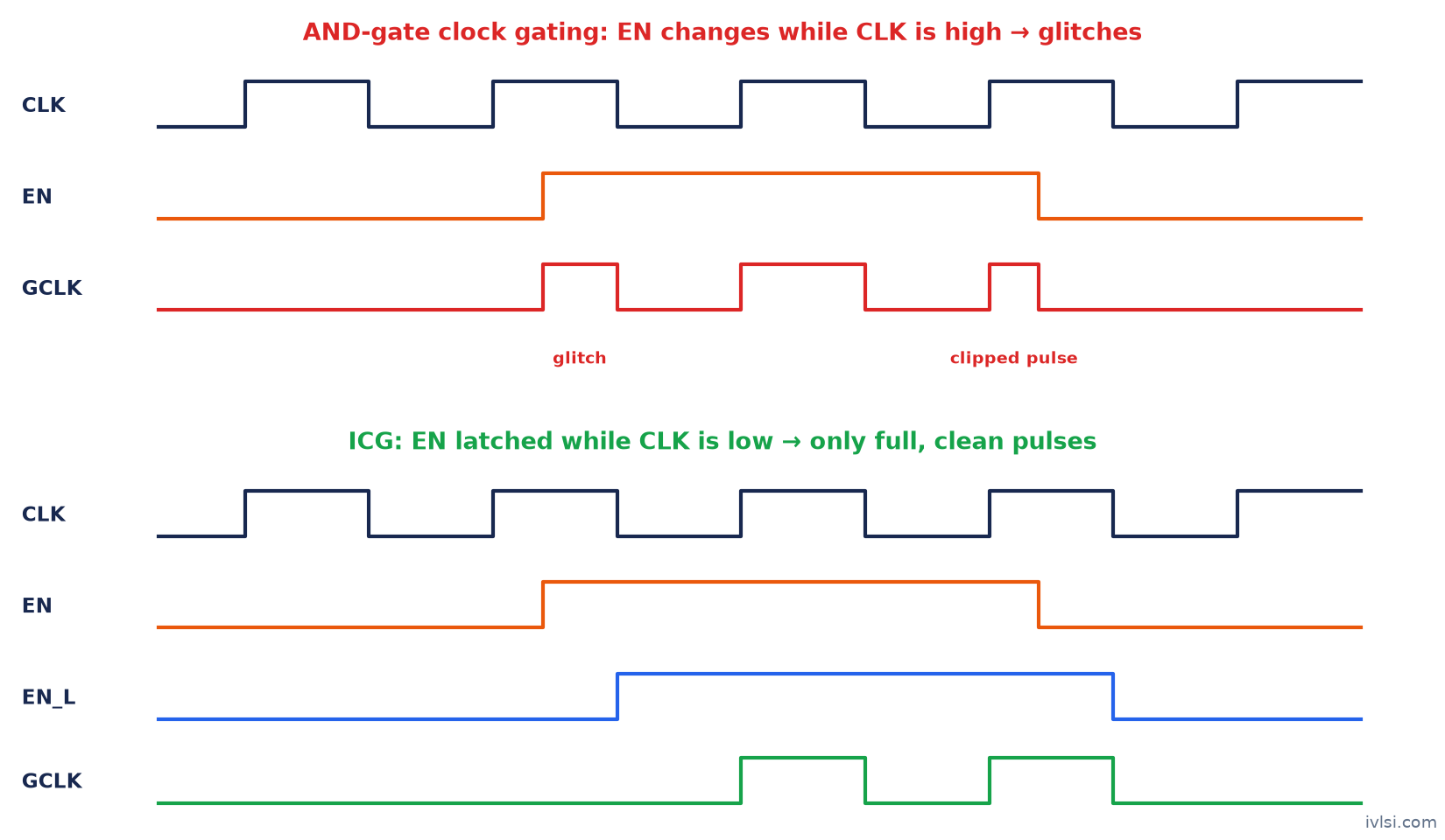
The simplest gating is GCLK = CLK AND EN. It works only if EN is stable for the whole time CLK is high. If EN changes while CLK is high, the output produces a shortened pulse (a glitch) or clips a pulse. A glitch on a clock can falsely trigger flip-flops or violate their minimum pulse width – a functional failure, not just a timing issue.
Enable signals usually come from flip-flops clocked on the rising edge, plus some logic, so they naturally change shortly after the rising edge – exactly when CLK is high. A plain AND gate is therefore unsafe for positive-edge flops.
Integrated Clock Gating (ICG) Cell
An ICG cell solves the glitch problem by adding a latch in front of the AND gate:
- A negative-level latch (transparent while CLK is low) samples the enable.
- The latched enable (EN_L) is ANDed with CLK to produce the gated clock GCLK.
- While CLK is high, the latch is closed, so EN_L cannot change and GCLK cannot glitch.
- A test enable (TE / SE) input is ORed with EN so that during scan test the clock always reaches the flops.
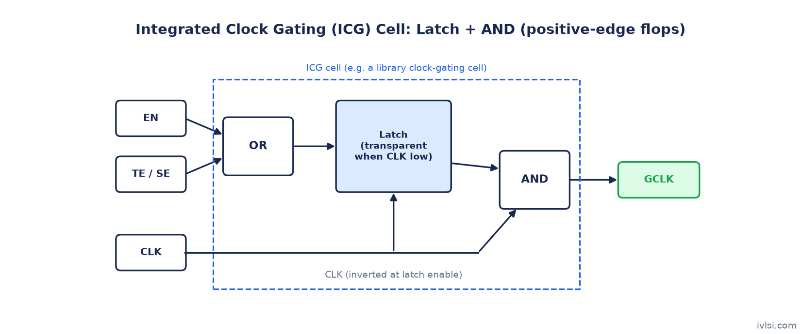
For negative-edge flops (or when the idle state of the gated clock should be high), the dual structure is used: a positive latch with an OR gate. Integrating the latch and gate into a single library cell lets the library characterise the internal timing precisely and lets tools recognise it as a clock-gating cell during CTS and STA.
| Aspect | AND/OR-gate gating | Latch-based ICG |
|---|---|---|
| Glitch-free | Only if EN is stable during the active phase | Yes, by construction |
| Timing check | Clock gating setup/hold on gate inputs | Setup/hold of EN relative to ICG CK pin |
| Area | Smallest | Slightly larger (latch + gate) |
| Scan/test support | Needs extra logic | Built-in TE/SE pin |
| Usage | Rare, special cases | Standard in synthesis and CTS flows |
Clock Gating Timing Checks
Because the enable controls a clock, STA performs clock gating checks on it. For an ICG cell, the library defines setup and hold constraints of EN relative to the ICG’s clock pin, so the check looks like a normal setup/hold check where the endpoint is the ICG enable pin. For a plain AND gate, STA infers a clock gating check: the enable must be stable before the rising edge (setup) and must not change until after the falling edge (hold) of the clock at the gate input.
Worked Example: Clock Gating Setup Check
T = 2.0 ns. The enable is launched by a flip-flop FF_EN with clock latency 0.40 ns, clock-to-Q 0.10 ns, and enable logic of 1.10 ns (max). The ICG clock pin latency is 0.30 ns and its setup requirement is 0.10 ns.
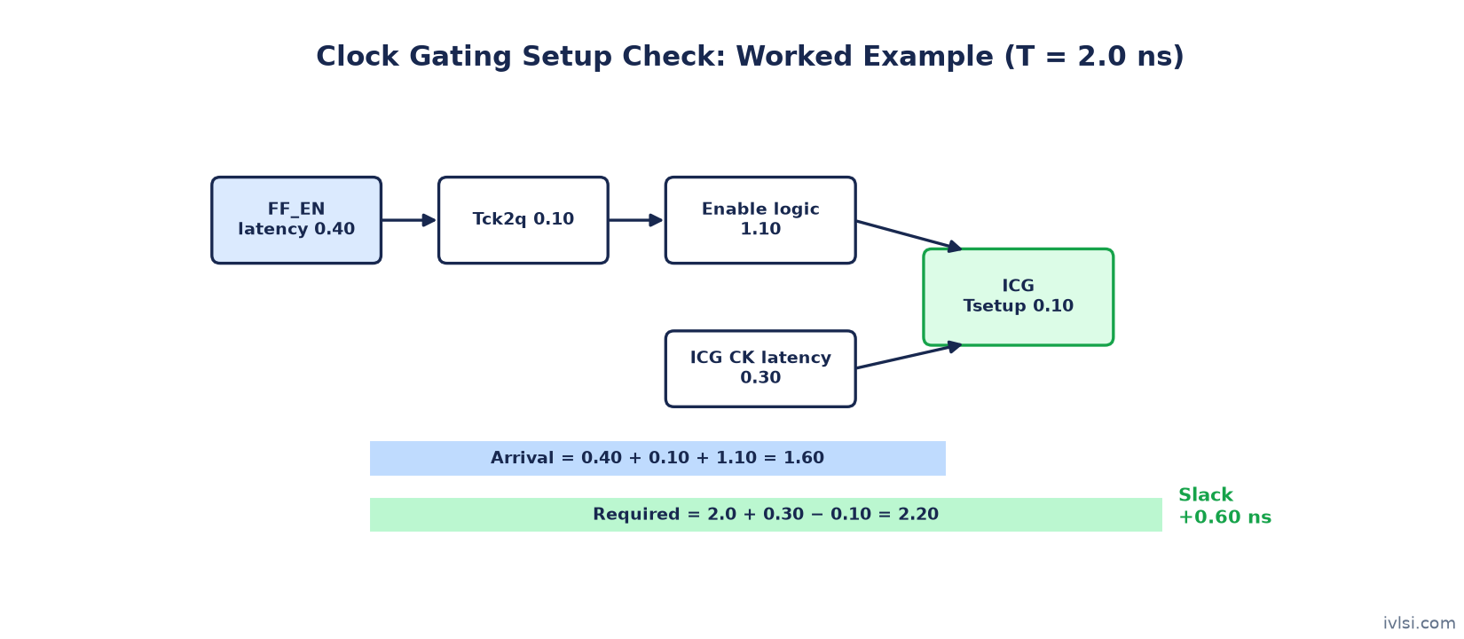
Arrival = 0.40 + 0.10 + 1.10 = 1.60 ns
Required = 2.0 + 0.30 − 0.10 = 2.20 ns
Setup slack = 2.20 − 1.60 = +0.60 ns
Worked Example: Clock Gating Hold Check
Same path with minimum delays: clock-to-Q 0.10 ns and minimum enable logic 0.05 ns; ICG hold requirement 0.05 ns.
Arrival = 0.40 + 0.10 + 0.05 = 0.55 ns. Required = 0.30 + 0.05 = 0.35 ns. Hold slack = 0.55 − 0.35 = +0.20 ns.
Notice the ICG clock pin has smaller latency (0.30 ns) than the flip-flops it eventually drives, because it sits higher in the clock tree. That early clock makes the enable setup check tighter – a common source of clock gating setup violations, discussed next. The general setup/hold equations are explained in Setup and Hold Violations and Static Timing Analysis (STA) in VLSI.
ICG Placement Trade-off: Power vs Timing
| ICG position | Power | Enable timing |
|---|---|---|
| Close to the clock root | More saving: a larger part of the clock tree is gated | Harder: ICG clock arrives early, so less time for the enable |
| Close to the gated flops | Less saving: tree above the ICG keeps toggling | Easier: ICG clock latency similar to flops |
Implementation tools balance this automatically, but it explains common fixes for clock gating violations:
- Clone the ICG and place copies closer to their flops (more latency at the ICG clock pin, more time for EN).
- Move the ICG down the clock tree, or allow CTS to treat the ICG as a balancing point appropriately.
- Optimise the enable path – upsize, restructure, or move the enable flip-flop closer to the ICG.
- Merge ICGs with identical enables to save area and power when timing allows.
- Use useful skew carefully on the enable-launching flop; see Useful Skew.
Clock Gating in the Implementation Flow
- RTL – designers write enable conditions (e.g.
if (en) q <= d;); see RTL Quality Effect on Synthesis. - Synthesis – the tool replaces enable muxes with ICG cells, usually for register banks above a minimum bit-width so the ICG overhead is worth it, and connects TE to the scan enable. See Synthesis Overview and Inputs.
- Placement – ICGs are placed near their fanout, cloned or merged based on timing.
- CTS – ICGs are part of the clock tree; the tool builds the tree through them and balances latency to the gated sinks. See Clock Tree Synthesis (CTS) and CTS Spec File.
- Sign-off STA – clock gating setup/hold checks are verified across all corners, together with minimum pulse width on gated clocks.
Types of Clock Gating
| Type | Granularity | Example |
|---|---|---|
| Fine-grained (register-level) | Small register groups | ICG per register bank with a common enable |
| Coarse-grained (block-level) | Whole module or subsystem | Gating the clock to an idle IP block |
| Multi-level | ICG driving other ICGs | Block-level ICG followed by register-level ICGs |
Clock gating reduces dynamic power only. To cut leakage in idle blocks, it is combined with power gating; see Power Switch Cell Placement.
Clock Gating Interview Questions
Q1. Why is a latch used inside an ICG cell?
To hold the enable stable while the clock is high, preventing glitches on the gated clock.
Q2. Why is a negative latch used for positive-edge flops?
The enable changes after rising edges; the negative latch is closed during the high phase, so changes only pass through during the low phase when the AND output is low anyway.
Q3. What is the purpose of the test enable pin?
To force the clock on during scan test so that all flops can shift, regardless of the functional enable.
Q4. Why are clock gating setup violations common?
The ICG sits higher in the clock tree, so its clock arrives earlier than the flops that launch the enable, leaving less time for the enable path.
Q5. Does clock gating reduce leakage power?
No, it reduces dynamic power. Leakage is reduced with techniques like power gating or high-Vt cells.
Q6. Why not gate every single flip-flop?
Each ICG has area, power and timing overhead; gating very small register groups may cost more than it saves.
Q7. What is the difference between clock gating and power gating?
Clock gating stops the clock (dynamic power); power gating switches off the supply (leakage power) and needs isolation and retention.
Q8. What check does STA do on an AND-gate clock gate?
A clock gating check: the enable must be stable before the rising edge and not change until after the falling edge of the clock at the gate.
FAQ
What is clock gating in VLSI?
It is a low-power technique that stops the clock to registers when they do not need to update, reducing dynamic power in the flops and the clock tree.
What is an integrated clock gating (ICG) cell?
A library cell that combines a latch and an AND (or OR) gate, plus a test enable, to gate a clock without glitches.
How much power does clock gating save?
It depends on how often the gated logic is idle and how much clock capacitance is gated; the saving is roughly proportional to the fraction of cycles the clock is turned off, minus the ICG overhead.
How do you fix clock gating setup violations?
Clone or move the ICG closer to its flops, optimise the enable logic, or adjust skew on the enable-launching flop.
Conclusion
Clock gating is the first line of defence against dynamic power, and the ICG cell makes it safe by latching the enable. Understand the glitch problem, the ICG structure, the clock gating setup and hold checks and the placement trade-off, and you will be able to debug gating issues in any flow. Continue with Time Borrowing (Cycle Stealing) for another latch-based timing concept.