

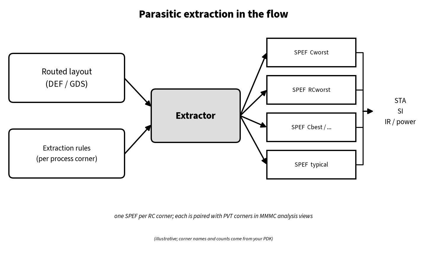
A path can show +40 ps of slack after placement and fail by 15 ps after routing, and nothing in the netlist has changed. The difference is the wires. Before routing, the tools estimate wire resistance and capacitance. After routing, parasitic extraction measures them from the real geometry and writes them into a SPEF file, and that file decides the sign-off timing, signal integrity and much of the power numbers. If the extraction is wrong, or the SPEF does not annotate properly, every report built on it is wrong too.
This guide covers parasitic extraction for physical design and STA engineers: what the extractor models, RC corners, how to read a SPEF file, how STA uses the data, worked examples, common problems and a debug order. The worked examples are illustrative: the numbers show the method and are not taken from any foundry, library or project. Real extraction rules, layer stacks and corner definitions come from your PDK and are not shown here. Command snippets are simplified sketches. Related reading on iVLSI: Static Timing Analysis (STA) in VLSI, Crosstalk in VLSI, MMMC in STA and OCV, AOCV and POCV in STA.
What is parasitic extraction?
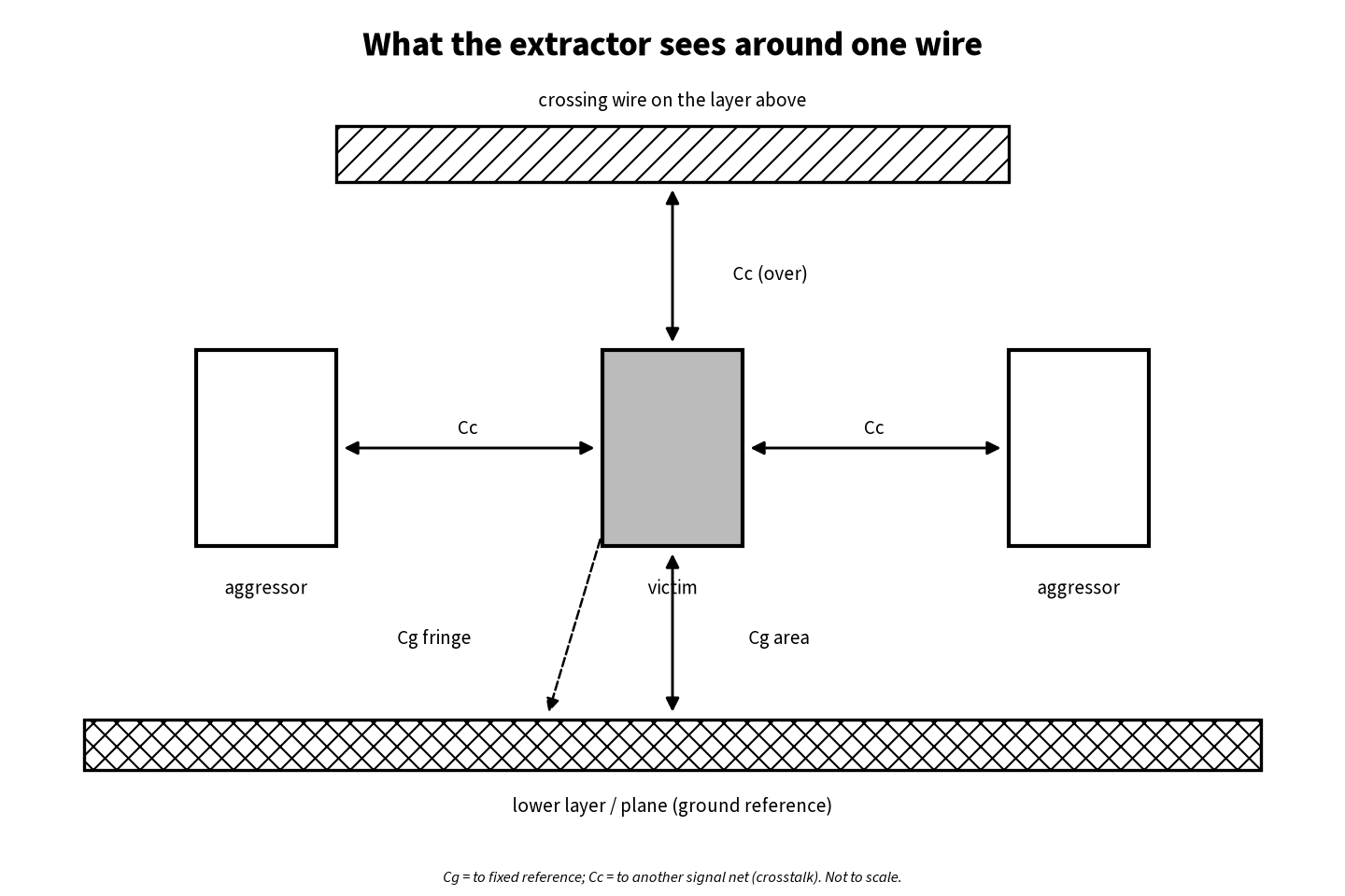
Every routed wire is a resistor and a capacitor that nobody drew on purpose. These unwanted elements are called parasitics. Extraction turns layout geometry into an electrical network with three kinds of element:
- Resistance (R) of wire segments and vias. It depends on the metal’s sheet resistance, the wire width and length, the number of via cuts and the temperature.
- Ground capacitance (Cg) from a wire to layers or substrate that are treated as fixed potential: area capacitance to the layer below or above, plus fringe capacitance from the wire’s sidewalls.
- Coupling capacitance (Cc) between two signal nets running side by side or crossing on nearby layers. Cc is the source of crosstalk delta delay and noise glitches.
For digital block timing, the RC network is the model; inductance is analysed separately where needed.
As nodes shrink, wires get narrower and sit closer together, so resistance per micron rises and more of the capacitance is sidewall coupling. Extraction accuracy becomes a sign-off topic.
Where extraction sits in the flow
Parasitics are estimated or extracted at several points, with rising accuracy:
| Stage | How RC is obtained | Typical use |
|---|---|---|
| Synthesis / placement | Wire-load models or placement-based estimates from net bounding boxes | Early optimisation; trends only |
| Pre-route (after CTS) | Global or trial routing plus per-layer RC estimates | Optimisation and CTS balancing before detailed routing |
| Post-route, in the P&R tool | Built-in extractor on detailed routes, tuned for speed | Post-route optimisation and ECO loops |
| Sign-off | Stand-alone sign-off extractor using rules calibrated against a field solver | Final STA, SI, IR and power sign-off |
The gap between these stages is called correlation. A flow is healthy when pre-route timing predicts post-route timing well, and when the P&R extractor agrees with the sign-off extractor closely enough that fixes made inside P&R hold up at sign-off.
What the extractor models
A full-chip field solve would be far too slow, so extractors work like this:
- The process team describes the metal stack: layer thicknesses, dielectric constants, wire width and spacing biases, and how these vary across corners.
- A field solver computes R and C for many small test patterns (a wire over a plane, a wire between two neighbours, a wire under another layer, and so on).
- The results are stored as tables or fitted equations in an extraction rules file (also called an RC technology file).
- During extraction, the tool breaks every routed net into segments, looks at each segment’s context (neighbours on the same layer, layers above and below) and looks up R and C from the tables.
The open-source OpenRCX extractor in OpenROAD documents this approach clearly: it extracts R and C from coupling distance and the over/under track context, interpolating on measurements stored in an Extraction Rules file generated once per process node and corner. Its controls include how many tracks of lateral context to consider, how many layers of vertical context to use, and a coupling threshold below which small coupling capacitors are grounded.
Things that change the answer in practice:
- Metal fill. Dummy fill near a wire adds capacitance. Sign-off extraction must either include the real fill or model it, and the P&R estimate should account for it, or post-fill timing will drift.
- Width and thickness variation. Wires drawn at the same width print differently depending on density and neighbours. Rules files include these effects per corner.
- Via resistance. Single-cut vias on long, high-current or critical nets add noticeable resistance. Multi-cut vias and via pillars reduce it.
- Temperature. Metal resistance increases with temperature, so the extraction temperature must match the analysis corner.
RC corners
Process variation changes wire width, thickness and dielectric height, and these do not move R and C in the same direction. A wider, thicker wire has lower R but higher C. So extraction is run at several RC corners. Names vary between PDKs and tools, but the common set is:
| RC corner | What is pushed | Usually worst for |
|---|---|---|
| Cworst (Cmax) | Highest capacitance | Short, load-dominated nets; often hold at fast PVT and max cap |
| Cbest (Cmin) | Lowest capacitance | Hold checks where data must not arrive too early |
| RCworst | Highest R×C product | Long, resistive nets; often setup on long routes |
| RCbest | Lowest R×C product | Hold on long nets |
| Typical | Nominal | Power analysis and reference |
Which corner is worst for a given path is not obvious. A path made of short nets driven by small cells is limited by capacitance, while a path with long nets on thin lower metals is limited by resistance. So sign-off pairs RC corners with PVT corners in an MMMC setup as your PDK and methodology require; “setup at RCworst only” is a risk, not a rule.
How STA uses parasitics
STA tools do not simulate the full RC network for every arc. They:
- Read the SPEF and attach each net’s RC network to the matching net in the netlist.
- Add pin capacitance from Liberty to the sink nodes, unless the SPEF says pin caps are already included.
- Reduce the network for delay calculation: the driver sees an effective capacitance (smaller than the total, because resistance shields far capacitance), and each sink gets its own wire delay and slew.
- Handle coupling in one of two ways. In a plain timing run, coupling capacitors can be grounded (treated as Cg). In an SI run, they are kept so the tool can compute delta delay and noise from aggressor timing windows.
The open-source OpenSTA read_spef command, for example, has a -keep_capacitive_coupling option to keep coupling caps instead of converting them to grounded caps, and a -coupling_reduction_factor (default 1.0) applied when networks are reduced. Worked example B shows why grounding Cc hides the worst case.
Reading a SPEF file
SPEF (Standard Parasitic Exchange Format) is the IEEE standard text format for passing extracted parasitics between tools. It is specified within IEEE 1481 (the current edition is IEEE 1481-2019, Integrated Circuit Open Library Architecture). A SPEF file has a header, an optional name map, optional ports, and then one section per net.
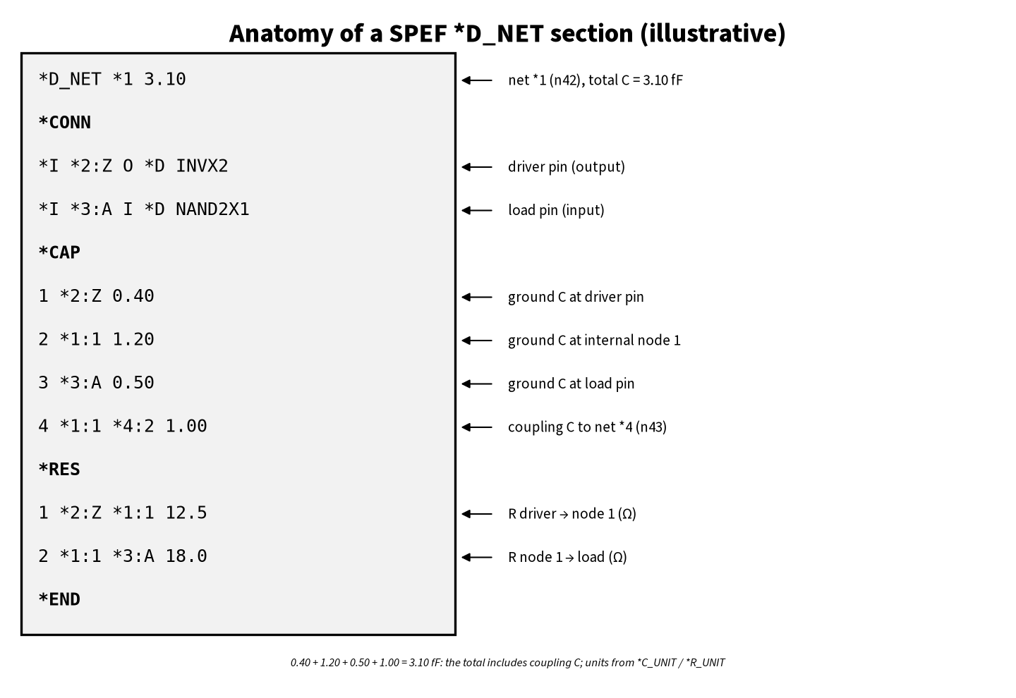
Here is a short, illustrative example for one net. Real files are generated by the extractor and are often several gigabytes for a large block.
*SPEF "IEEE 1481-1998"
*DESIGN "blk_top"
*DATE "illustrative"
*VENDOR "illustrative"
*PROGRAM "illustrative"
*VERSION "1.0"
*DESIGN_FLOW "PIN_CAP NONE"
*DIVIDER /
*DELIMITER :
*BUS_DELIMITER [ ]
*T_UNIT 1 NS
*C_UNIT 1 FF
*R_UNIT 1 OHM
*L_UNIT 1 HENRY

*NAME_MAP
*1 n42
*2 u1
*3 u2
*4 n43

*D_NET *1 3.10
*CONN
*I *2:Z O *D INVX2
*I *3:A I *D NAND2X1
*CAP
1 *2:Z 0.40
2 *1:1 1.20
3 *3:A 0.50
4 *1:1 *4:2 1.00
*RES
1 *2:Z *1:1 12.5
2 *1:1 *3:A 18.0
*END
How to read it:
- Units come first (here fF and ohms). A
PF/FFmix-up is a classic, silent mistake. *DIVIDER,*DELIMITERand*BUS_DELIMITERdefine the hierarchy separator, the pin separator and bus brackets. If these do not match how the netlist names objects, nets fail to annotate.*NAME_MAPreplaces long names with short indices such as*1to keep the file smaller.*D_NET *1 3.10starts a detailed net (n42) with total capacitance 3.10 fF. The total is the sum of every capacitor listed for the net, including coupling: 0.40 + 1.20 + 0.50 + 1.00 = 3.10.*CONNlists the net’s connections.*Imarks an instance pin with its direction (Ooutput,Iinput), and*Dnames the driving cell type.*Pwould mark a top-level port.*CAPlists capacitors. A line with one node is a ground capacitor (2 *1:1 1.20is 1.20 fF at internal node 1). A line with two nodes is a coupling capacitor (4 *1:1 *4:2 1.00couples node 1 ofn42to node 2 ofn43). The same coupling capacitor also appears inn43‘s section.*RESlists resistors between nodes, forming the RC tree from the driver pin to each sink pin.
Sign-off STA and SI flows normally use these detailed (*D_NET) networks rather than reduced (*R_NET) models.
Worked example A: Elmore delay from a SPEF net (illustrative)
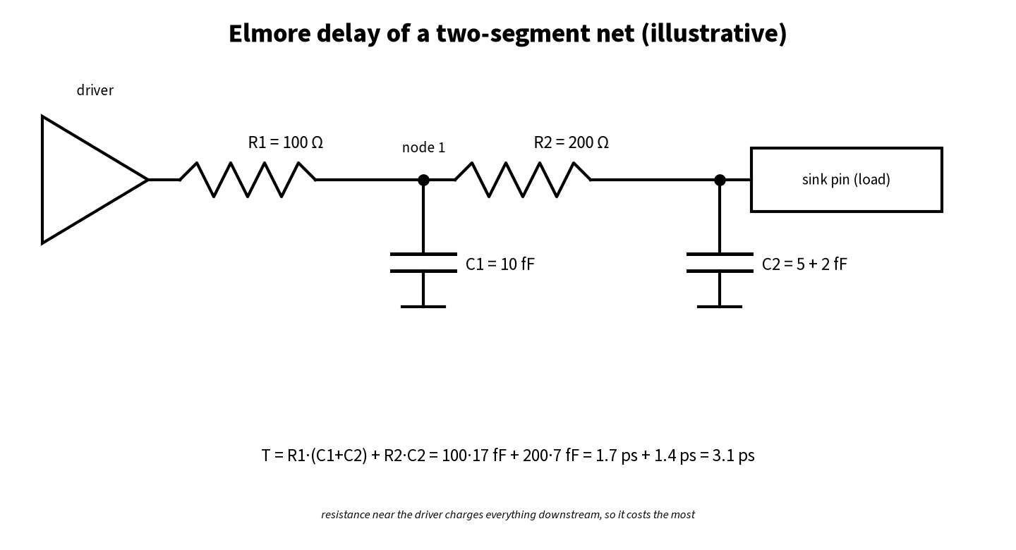
The Elmore delay is a simple first-order estimate of wire delay in an RC tree. For each resistor on the path from driver to sink, multiply its resistance by all the capacitance downstream of it, then add the products. Sign-off tools use more accurate methods, but Elmore is useful for sanity checks and is a favourite interview question.
Take a two-segment net (illustrative values):
- R1 = 100 Ω from the driver pin to node 1; capacitance at node 1, C1 = 10 fF
- R2 = 200 Ω from node 1 to the sink; capacitance at the sink, C2 = 5 fF of wire + 2 fF of sink pin = 7 fF
Downstream of R1 is C1 + C2 = 17 fF. Downstream of R2 is only C2 = 7 fF.
Elmore delay = R1 × (C1 + C2) + R2 × C2 = 100 Ω × 17 fF + 200 Ω × 7 fF = 1.7 ps + 1.4 ps = 3.1 ps
(100 Ω × 17 fF = 1,700 × 10⁻¹⁵ s = 1.7 ps.)
Resistance near the driver costs the most, because it charges everything downstream. And if the router moves R2’s segment from an upper metal to a thin lower metal and R2 becomes 600 Ω, the second term triples to 4.2 ps and the wire delay becomes 5.9 ps. The netlist did not change; only the layer did.
Worked example B: why coupling capacitance cannot just be grounded (illustrative)
A victim net has Cg = 8 fF to ground and Cc = 4 fF to one neighbouring aggressor. Using a simple switch-factor (Miller) model:
| Aggressor behaviour | Effective capacitance on victim | Value |
|---|---|---|
| Quiet (not switching) | Cg + Cc | 12 fF |
| Switching in the same direction | Cg + 0 × Cc | 8 fF |
| Switching in the opposite direction | Cg + 2 × Cc | 16 fF |
If coupling is simply grounded at a factor of 1, the victim always sees 12 fF. But in the opposite-switching case it really sees 16 fF, which is a third more load, and in the same-direction case only 8 fF, which can make a hold path faster than expected. This is why SI analysis keeps Cc separate and uses aggressor timing windows: it adds positive delta delay to setup analysis and negative delta delay to hold analysis only where the switching can really overlap. The Crosstalk in VLSI and Signal Integrity and Crosstalk posts cover the fixes: spacing, shielding, layer changes and upsizing the victim driver.
Worked example C: pre-route vs post-route miscorrelation (illustrative)
After CTS, a register-to-register path reports +40 ps setup slack using global-route estimates. After detailed routing and extraction at the RCworst corner, it reports −15 ps. A 55 ps swing is worth understanding before fixing:
- Report the path in both runs and compare stage by stage. Here, the cell delays are within a few ps, but one net’s wire delay grew from 6 ps to 38 ps, and the sink slew degraded so the next cell got slower too.
- Inspect that net: its length, layers and vias. The global router planned it on upper metal, but congestion forced the detailed router to drop a long segment onto a thin lower layer through single-cut vias.
- Check the SPEF: the net’s total capacitance is close to the estimate, but its resistance is several times higher. This is a resistance problem, not a load problem.
- Fix the cause: put a layer-promotion constraint or a non-default rule (wider or double-cut) on the net, or insert a repeater. Then re-extract and recheck.
- Feed it back: if many nets show the same pattern, the pre-route RC scaling factors or congestion in that region need attention. Otherwise the next run will show the same surprise.
Common problems and fixes
| Symptom | Likely cause | Fix |
|---|---|---|
| Many nets reported as not annotated | Netlist and SPEF from different versions (for example, SPEF from before an ECO) | Re-extract from the final database; keep netlist and SPEF in lock-step |
| A few nets not annotated, all with escaped or bus names | Divider, delimiter or bus-bracket mismatch; escaped identifiers handled differently | Align naming settings between extractor and STA; check *DIVIDER and *BUS_DELIMITER |
| Timing far too optimistic everywhere | Wrong units, or pin caps counted zero times | Check *C_UNIT/*R_UNIT and the pin-cap setting |
| Timing far too pessimistic on every net | Pin caps counted twice (in SPEF and from Liberty) | Match the pin-cap setting in the reader to how the SPEF was written |
| Hold passes in P&R but fails at sign-off | Hold checked only at Cworst; Cbest or RCbest corner not analysed | Add the missing RC corners to the MMMC view list |
| P&R and sign-off timing disagree on many nets | Different rules files or fill assumptions between extractors | Use matching rules versions; include or model fill in both |
| Large SI delta delay on a few nets | Long parallel runs next to switching aggressors | Spacing, shielding, layer change, or upsizing the victim driver |
| Post-route wire delay much larger than pre-route | Detours or lower-metal routing from congestion; single-cut vias | Layer promotion, NDRs, buffering, congestion relief |
Debug flowchart: fixing extraction and SPEF issues
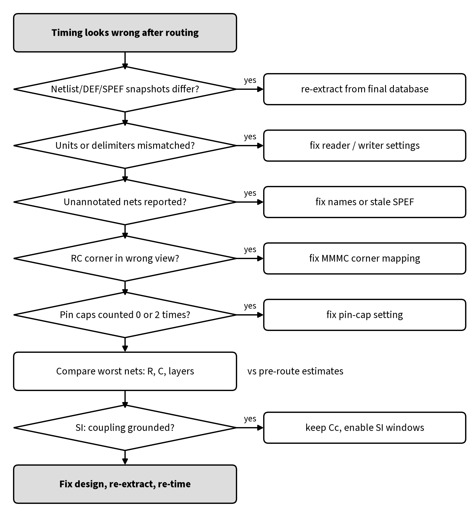
- Versions. Are the netlist, DEF and SPEF all from the same database snapshot?
- Header. Are the units, divider and bus delimiters what the reader expects?
- Annotation. Run the tool’s annotation report and get unannotated nets to zero (or to a list you understand, such as tie-offs and nets inside black boxes).
- Corners. Is each SPEF loaded into the analysis view with the matching RC corner and temperature?
- Pin caps. Are pin capacitances counted exactly once?
- Suspicious nets. Compare R, C and layer usage against pre-route for the worst offenders.
- Coupling. For SI sign-off, are coupling caps kept, and are aggressor timing windows available?
- Fix and re-extract. Only now change the design, then extract again; never reuse an old SPEF after an ECO.
A note on tool hints
Commercial tools have their own commands, so follow your vendor’s documentation. In the open-source flow:
# OpenROAD with OpenRCX (sketch; see the OpenROAD "Parasitics Extraction" docs)
set_extraction_rules_file rules/rcx_patterns.rules   ;# per process corner
extract_parasitics
write_spef blk_top.spef

# OpenSTA (sketch)
read_liberty  lib/stdcells.lib
read_verilog  blk_top.v
link_design   blk_top
read_sdc      blk_top.sdc
read_spef     blk_top.spef
report_parasitic_annotation     ;# check for nets without parasitics
report_checks -path_delay max
OpenRCX also has diff_spef to compare its result with a reference SPEF, which is handy for correlation checks. Option names change between releases, so check the current documentation before you script around them.
Interview Q&As
Q1. What is parasitic extraction, and why is it needed?
It computes the resistance and capacitance of routed wires and vias from the layout geometry. Delay calculation, SI, IR and power analysis need these values. Without them, timing would only count cell delays and would be wrong.
Q2. What is the difference between ground capacitance and coupling capacitance?
Ground capacitance connects a net to a fixed-potential reference. Coupling capacitance connects two signal nets, so its effect depends on what the other net is doing. Coupling causes crosstalk delta delay and noise.
Q3. What are the main sections of a SPEF file?
Header (including units and naming delimiters), an optional name map, optional ports, and per-net sections. Each *D_NET section has *CONN, *CAP, *RES and *END.
Q4. Why do we have Cworst and RCworst corners?
Because process variation moves R and C in opposite directions. Short, load-dominated nets are worst at maximum C. Long, resistive nets are worst at maximum R×C. Both must be checked.
Q5. How do you compute Elmore delay?
For each resistor from driver to sink, multiply its resistance by the total capacitance downstream and add the products. With R1 = 100 Ω, R2 = 200 Ω, C1 = 10 fF and C2 = 7 fF, it is 100 × 17 fF + 200 × 7 fF = 3.1 ps (illustrative).
Q6. Your STA shows thousands of unannotated nets after reading the SPEF. What do you check?
That the SPEF and netlist come from the same version, that hierarchy dividers and bus delimiters match, and that escaped names are handled the same way. Then re-extract if the SPEF is stale.
For more practice, see Routing Interview Questions and Answers and Static Timing Analysis (STA) in VLSI.
FAQ
Is SPEF the same as DSPF?
No. Both carry parasitics, but SPEF is the IEEE standard format that digital STA and SI tools read. DSPF is a SPICE-oriented format often used for transistor-level and analog simulation.
Why is the P&R extractor different from the sign-off extractor?
The P&R extractor is tuned for speed inside optimisation loops. The sign-off extractor is slower and calibrated more closely to field-solver results. A good flow keeps them correlated so fixes made in P&R hold at sign-off.
Summary
- Parasitic extraction turns routed geometry into R, ground C and coupling C, and writes them to SPEF for STA, SI and power tools.
- Extractors use rules files calibrated with a field solver, plus each wire’s lateral and vertical context. Fill, width variation, vias and temperature all matter.
- RC corners (Cworst, Cbest, RCworst, RCbest, typical) cover variation that moves R and C in opposite directions; pair them with PVT corners in MMMC.
- Learn to read a
*D_NETsection: total C, connections, ground and coupling caps, and the resistor tree. - When timing looks wrong after routing, check versions, units, naming, annotation, corners and pin caps before changing the design.
References
- IEEE Standards Association, “IEEE 1481-2019 – IEEE Standard for Integrated Circuit (IC) Open Library Architecture (OLA)” (includes the SPEF specification): https://standards.ieee.org/ieee/1481/7651/
- OpenROAD documentation, “Parasitics Extraction” (OpenRCX:
extract_parasitics,write_spef,diff_spef, Extraction Rules file): https://openroad.readthedocs.io/en/latest/main/src/rcx/README.html - OpenSTA source,
read_spefcommand help (-keep_capacitive_coupling,-coupling_reduction_factor,-pin_cap_included,report_parasitic_annotation): https://github.com/parallaxsw/OpenSTA/blob/master/parasitics/Parasitics.tcl - Related iVLSI posts: Routing in VLSI Physical Design, Understanding Metal Layers, Design Exchange Format (DEF), Timing Library (.lib), Setup and Hold Violations, Design Rule Violations (DRVs)